ESSENTIAL ELECTRONICS FOR AS –LEVEL BY CHRIS BARNES
PhD Eng., MCIEA
Preface
Many students these days embark on an A-level
Electronics Course without any prior knowledge whatsoever. As a crucially helpful asset, the author has
more than twenty five years experience in Electronics at Industrial and Teaching
Levels and Examining Levels
This book aims to provide the essential
elements of knowledge for AS-level.
It is particularly suited to the AQA
Electronics Syllabus but will also have value as a general reference text. It will also have
value for GCSE Electronics courses and GCSE Design Technology Electronics
Products courses.
Nothing is more daunting than opening a book on
Electronics and seeing its earliest pages and pages crammed full of calculation
strewn diagrams before you have mastered the basics. The early chapters of this book will
therefore, assuming no prior knowledge, and address the very simplest aspects
of Electricity and Electronics.
Firm foundations, however, will be quickly
built upon leading to theoretical and practical examples covering the entire AS
syllabus. It goes without saying then the parts of this book could also be used
as a reference manual for other vocational and non-vocational courses in
Electricity, Radio and Electronics, such as aspects of B-TECH Level 2 and 3
Engineering.
If you intend to study Electronics at A2 level,
the sister text Essential Electronics for A2 level will be an additional
invaluable asset.
CHAPTER ONE:
SOURCES OF ELECTRICITY
Electronic gismos are ubiquitous in our world, they all around us. All these devices contain electronic systems
and sub-systems, some with simple circuitry, some with very complex circuitry
but all with one thing in common, they need a source of electricity to make
them work. This electricity is converted into signals in the equipment which
either process (change in some way) information and/or direct its flow from one
point to another.
When we think of sources of electricity we would probably think firstly
of the power outlet in our front room
where the TV or Hi-fi is plugged in and secondly we would think of a battery,
maybe in car or digital camera or T.V
remote or whatever and we would in one sense be right. In another sense we could think that everything
around us contains some electricity!
Atoms that we might vaguely remember from our Chemistry lessons make up
everything and these in turn are made from ‘electrical’ particles. That is
particles which carry an electric charge. The tiniest of these and the ones
which move inside wires and electric circuits are called Electrons.
There are subtle differences however between electricity from the mains
and a battery of whatever type, wet and containing acid as in car, or dry and
containing a special jelly-like material as in say our digital camera.
Electricity
from batteries
Electricity from batteries is called D.C. or direct current and here the
electrons can only flow in one direction through the circuit from out from one
pole of the battery, called the negative and back in to another pole of the
battery called the positive.
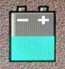 +
+ -
-
Fig 1.1
Practical battery Circuit symbol
of battery
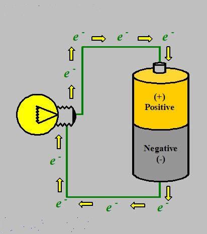
Fig 1.2 Practical
diagram showing flow of electrons
Way back in history people were making batteries before they really knew
about Electrons. They were very
misguided but in their infinite wisdom decreed that D.C Electricity flowed in
exactly the opposite way which we now know to be true. In other words they
defined what is still known to this day as Conventional Current Flow.
Conventional current flow was deemed to go from the positive pole of a
battery, given the symbol (+ or +vet) to the negative pole, given the symbol (–
or –vet). Of course, electrical current only ever flows when there is some kind
of electrical connection or circuit joining these two poles of the
battery. Circuits can be drawn as real
pictures of the components used or alternatively and more conveniently
diagrammatically as circuit or schematic diagrams. A range of symbols is used in circuit
diagrams. A suitable circuit might
contain a component known as a resistor, given the symbol R which has a property known as resistance which restricts or cuts down current flow and gets warm
or hot in the process. In Electronics a
flow of current is normally denoted by the symbol I and has units of Amperes (often abbreviated to Amps).
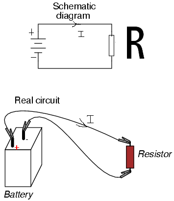
Fig 1.3
Note the difference between wire
in the practical set up diagram which may be curved or straight or take
whatever route and the diagrammatic representation of wires in the circuit or
schematic diagram which are by convention always shown as straight lines.
If wires from a battery are short circuited or joined together without a
series resistor or bulb as a load then excessive current may flow and they may
get very hot or even start a fire if the battery is big enough. This is a
potentially dangerous situation. Wires alone have practically zero resistance
to the flow of an electric current.
On the other hand if there is break in a circuit has a break in it no
current flows. A break in a circuit can be thought of as like an infinitely
high resistance. A break is sometimes
called an open circuit.
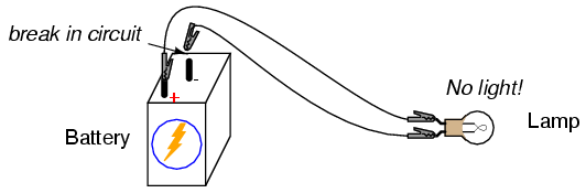
Fig 1.4 The open circuit
When the battery is connected in a
circuit it is doing work. Its terminal voltage (V) measured in units of volts
is pushing electrons through the
circuit. With an open circuit or no flow of electrons,
the entire potential (voltage) of the battery is available across the break,
waiting for the opportunity of a connection to bridge across that break and
permit electron flow again. In an open circuit the break in the continuity of
the circuit prevents current throughout. All it takes is a single break in
continuity to “open” a circuit. Once any breaks have been connected once again
and the continuity of the circuit re-established, it is known as a closed circuit.
We now have the basis for switching lamps on and off by remote switches. Because any break in a circuit’s continuity results in current stopping throughout the entire circuit, we can use a device designed to intentionally break that continuity (called a switch), mounted at any convenient location that we can run wires to, to control the flow of electrons in the circuit:
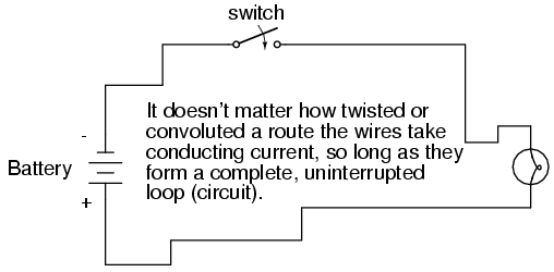
Figure 1.5 Wiring routes
This is how a switch mounted on the wall of a house can control a lamp that is mounted down a long hallway, or even in another room, far away from the switch. The switch itself is constructed of a pair of conductive contacts (usually made of some kind of metal) forced together by a mechanical lever actuator or pushbutton. When the contacts touch each other, electrons are able to flow from one to the other and the circuit’s continuity is established; when the contacts are separated, electron flow from one to the other is prevented by the insulation of the air between, and the circuit’s continuity is broken.
Perhaps the best kind of switch to show for illustration of the basic principle is the “knife” switch:
A knife switch is nothing more than a conductive lever, free to pivot on a hinge, coming into physical contact with one or more stationary contact points which are also conductive. The switch shown in the above illustration is constructed on a porcelain base (an excellent insulating material), using copper (an excellent conductor) for the “blade” and contact points. The handle is plastic to insulate the operator’s hand from the conductive blade of the switch when opening or closing it.
Here is another type of knife switch, with two stationary contacts instead of one:
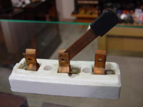
Figure 1.6 Changeover Knife Switch
The particular knife switch shown here has one “blade” but two stationary contacts, meaning that it can make or break more than one circuit. For now this is not terribly important to be aware of, just the basic concept of what a switch is and how it works.
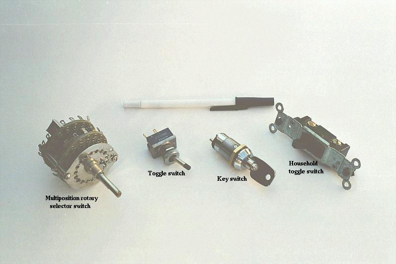
Knife switches are great for illustrating the basic principle of how a switch works, but they present distinct safety problems when used in high-power electric circuits. The exposed conductors in a knife switch make accidental contact with the circuit a distinct possibility and any sparking that may occur between the moving blade and the stationary contact is free to ignite any nearby flammable materials. Most modern switch designs have their moving conductors and contact points sealed inside an insulating case in order to mitigate these hazards. A photograph of a few modern switch types show how the switching mechanisms are much more concealed than with the knife design:
In keeping with the “open” and “closed” terminology of circuits, a switch that is making contact from one connection terminal to the other (example: a knife switch with the blade fully touching the stationary contact point) provides continuity for electrons to flow through, and is called a closed switch. Conversely, a switch that is breaking continuity (example: a knife switch with the blade not touching the stationary contact point) won’t allow electrons to pass through and is called an open switch. This terminology is often confusing to the new student of electronics, because the words “open” and “closed” are commonly understood in the context of a door, where “open” is equated with free passage and “closed” with blockage. With electrical switches, these terms have opposite meaning: “open” means no flow while “closed” means free passage of electrons.
Alternating
Current (A.C)
We have seen how batteries generate D.C. electricity. Imagine connecting a battery to a reversing
switch and then to a lamp or torch bulb. Each time the reversing switch was
operated, the flow of electricity through the circuit would be reversed. The
lamp would momentarily go on and off.
However if you could operate the reversing switch fast enough the lamp
would appear to be on all the time because you eye would not be able to respond
to the flickering changes in brightness.
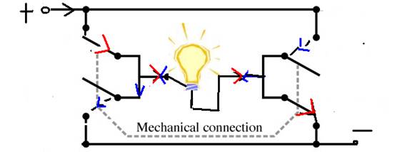
Figure 1.8 A.C. From reversing
circuit
The red arrows show electric current going through the bulb from left to
right (solid
lines on reversing switch) and
the blue arrows show the current having reversed direction through the bulb
from right to left as through the dashed lines on reversing switch) .
A.C. Electricity fro a Mains Outlet behaves in exactly this manner. A.C. electricity is generated from mechanical
machines called generators or alternators which employ coils of wire and
magnets. D.C. can also be generated from a mechanical machine of similar
construction known as a dynamo. With our
reversing switch the change in direction of the current flow would be very
sharp and abrupt but with most AC Electricity the change in direction of the
current flow is smooth and continuous and is called a sinusoid or sine wave
after the mathematical function that you will see on any scientific
calculator. A typical sine wave is
shown below , note the smooth variation of the voltage with time, the current
in the circuit reverses each time the line of the wave crosses zero.
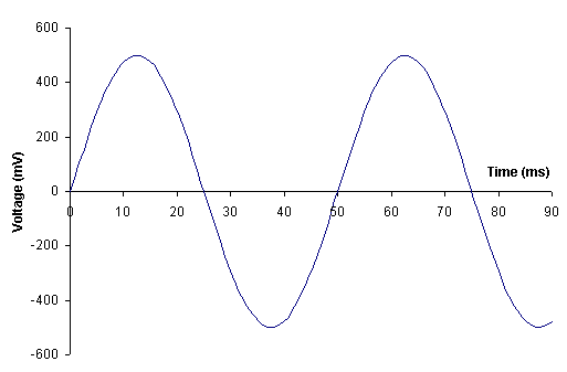
Figure 1.9 A.C. Sine wave
How fast
does electricity flow?
It may surprise you to know that electricity in wires flows almost as
fast as the speed of light! This is because wires, as with all electrical
conductors, are always full of electrons. The current from the battery merely
introduces extra electrons sequentially at one end of the wire and there is a
‘knock-on effect’ through the wire. If we were to follow the speed of any one
single injected electron it alone would be much slower.
There is a good analogy with marbles in a tube.
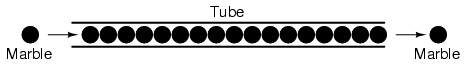
Figure 1.10 Marble-electron
analogy
Pushing the marble in at the left of the tube makes the marble on the
right drop out almost instantaneously but there is a considerable delay before
the marble on the left drops out at the right. In fact, simplistically, as
there are seventeen marbles in the tube we could say this delay is the transit
time for all seventeen marbles plus the loading time for the tube to be
refilled.
REVIEW
· Batteries chemically generate D.C. electricity
· Electrons are found in the atoms of all materials
· An electric current is a flow of electrons
· An electric potential or voltage does work in pushing electrons through a circuit
· Conventional current flows from positive to negative
· Resistance is the measure of opposition to electric current
· Resistors generate heat
· A short circuit is an electric circuit offering little or no resistance to the flow of electrons. Short circuits are dangerous with high voltage power sources because the high currents encountered can cause large amounts of heat energy to be released.
· An open circuit is one where the continuity has been broken by an interruption in the path for electrons to flow.
· A closed circuit is one that is complete, with good continuity throughout.
· A device designed to open or close a circuit under controlled conditions is called a switch.
· The terms “open” and “closed” refer to switches as well as entire circuits. An open switch is one without continuity: electrons cannot flow through it. A closed switch is one that provides a direct (low resistance) path for electrons to flow through.
· A.C Electricity may be simulated using a battery and very fast reversing switch.
· A.C. Electricity is usually generated using Electromagnetic machines called generators or alternators. Electricity generated in this way has a smooth variation of voltage with time known as a sine wave.
· An electric current in closed circuit is virtually instantaneous from the moment of switch- on, close to the speed of light, but single electrons drift more slowly.
·
·
·
·
·
·
·
CHAPTER 2: BASIC ELECTRICAL CALCULATIONS
Take our battery and resistor series circuit from the last chapter. The greater the battery voltage or terminal potential difference the more ability it has to drive current round the circuit. Thus the hotter the resistor gets. The voltage can be measured by an instrument known as a voltmeter which may be of moving coil or electronic (digital) construction. Likewise the current may be measured by an ammeter of either of the foregoing constructions. The heat generated or the power dissipated in the resistor is a function of the work done driving electrons through it.
The fundamental
equation linking Power (P) measured in
P= I x V
Or in words
using units
Some students find the memory mnemonic, involving a fictitious Welsh girls’ name useful; W= Ivy Watts. This helps them remember the equation for Power contains the product of I and V. A product is two numbers multiplied together.
Worked example.
A circuit has a battery with open circuit terminal voltage of 12 volts.
When connected to a bulb the battery voltage does not
significantly change and the current flowing through the bulb is 2 Amps. Calculate the power dissipated (used up) by
the bulb.
P=IxV P =
2x12 =24 Watts
Answer 24 Watts
Decimal Prefixes
Mathematics used in technology and engineering often uses very large numbers. Instead of writing or saying these numbers, we can use several types of shorthand.
Prefixes - A prefix is added to the front of a unit (e.g. length or mass ) as a multiplier. ‘Kilo’ always tell you to multiply by a thousand. 1 kilogram is 1000 grams.
Symbols - Long numbers also have symbols, ‘k’ stands for ‘kilo’ or 1000. Instead of writing 0.000001 meter we can write ‘ m ‘ which is one micron ( 1 millionth of a meter ). For example, an average human hair is 100 micron thick.
To abbreviate long numbers engineers often use exponents. This is a small number that tells you how many zeros the actual number contains. Many calculators now have an engineering function key that allows you to key in numbers with exponents and to manipulate them to solve problems. This avoids keying in - and possibly becoming confused by very long numbers.
These general situations of decimal prefixes and exponents often apply in Electronics we come across problems with smaller fractions of the fundamental or S.I. (International System) units which are decimal sub-divisions.
Sometimes we come across decimal multiples of S.I. units. These subdivisions and multiples are given special names and it is instructive to know and hopefully learn them at this stage.
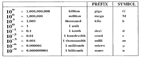
Figure 2.1 Decimal prefixes
Note that the exponent 100 has no prefix or symbol because it is merely 1 S.I. Unit.
Examples
One thousandth of a volt =
1/1000 volts = 10 -3 volt = 1 millivolt
1000 volts = 1 kilo-volt
One thousandth of an Amp = 1/1000 Amps = 10 -3 Amps
= 1 milliamp One millionth of an Amp
= 1/1000, 000 Amps = 10 -6 Amps
= 1 microamp Etc; etc.
It is very important to take decimal prefixes properly into account when calculated Power for example.
There are toe
possible approaches to problems. Either convert everything (both the volts and
amps) back to S.I. units with no prefix first OR if either is in ‘MILLI’ form
the answer will automatically be in ‘MILLI’ form OR if both are in ‘MILLI’
form, the answer will automatically be in MICRO form since 10 -3
x
10 -3 = 10 -6
WORKED EXAMPLES
1. A twelve volt battery drives a current of 2 mA through a circuit. Calculate the power dissipated by the circuit.
Either P= I xV P = 2x10-3 x 12 = 24 x 10-3 W = 24 milliwatts
OR P= 2 Milliamps x 12 Volts = 24 Milliwatts (automatically!)
2. A resistor in a complex circuit has 12 millivolts across it and a current of 12mAflowing through it both as measured by a very high resistance digital multi-meter. Calculate the power dissipated in the resistor.
Either P= I x V P = 12 x 10-3 x 12 x 10-3 = 144 x 10-6 W = 144 microwatts
OR P = 12 Milliamps x 12 Millivolts = 144 Microwatts (automatically!)
Note how either method admirably obtains the correct answer.
Ohm’s Law
“One microampere flowing in one ohm causes a one microvolt potential drop.”
Georg Simon Ohm
How voltage, current, and resistance are related
An electric circuit is formed when a conductive path is created to allow free electrons to continuously move. As we have seen this continuous movement of free electrons through the conductors of a circuit is called a current, and it is often referred to in terms of “flow,” just like the flow of a liquid through a hollow pipe.
The force motivating electrons to “flow” in a circuit is called voltage. Voltage is a specific measure of potential energy that is always relative between two points. When we speak of a certain amount of voltage being present in a circuit, we are referring to the measurement of how much potential energy exists to move electrons from one particular point in that circuit to another particular point. Without reference to two particular points, the term “voltage” has no meaning. As we have seen in one of the pervious worked examples such a pair of points could be the terminal ends of a resistor.
Free electrons tend to move through conductors with some degree of friction, or opposition to motion. As we saw in Chapter One, this opposition to motion is more properly called resistance. The amount of current in a circuit depends on the amount of voltage available to motivate the electrons, and also the amount of resistance in the circuit to oppose electron flow. Just like voltage, resistance is a quantity relative between two points. For this reason, the quantities of voltage and resistance are often stated as being “between” or “across” two points in a circuit.
: To be able to make meaningful statements about these quantities in circuits, we need to be able to describe their quantities in the same way that we might quantify mass, temperature, volume, length, or any other kind of physical quantity. For mass we might use the units of “pound” or “gram.” For temperature we might use degrees Fahrenheit or degrees Celsius. Here are the standard units of measurement for electrical current, voltage, and resistance
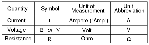
Figure 2.2 Electrical quantities
The “symbol” given for each quantity is the standard alphabetical letter used to represent that quantity in an algebraic equation. Standardized letters like these are common in the disciplines of physics and engineering, and are internationally recognized. The “unit abbreviation” for each quantity represents the alphabetical symbol used as a shorthand notation for its particular unit of measurement. The strange-looking “horseshoe” symbol is the capital Greek letter Ω, (omega).
In fact as we progress in Electronics, we will come to realize that each and every unit of measurement is named after a famous experimenter in electricity or magnetism: for instance in the table above, the amp after the Frenchman Andre M. Ampere, the volt after the Italian Alessandro Volta, and the ohm after the German Georg Simon Ohm.
The mathematical symbol for each quantity is meaningful as well. The “R” for resistance and the “V” for voltage are both self-explanatory, whereas “I” for current seems a bit weird. The “I” is thought to have been meant to represent “Intensity” (of electron flow), and the other symbol for voltage, “E,” stands for “Electromotive force.” From what research I’ve been able to do, there seems to be some dispute over the meaning of “I.” The symbols “E” and “V” are interchangeable for the most part, although some texts reserve “E” to represent voltage across a source (such as a battery or generator) and “V” to represent voltage across anything else.
Strictly speaking capital letters are used where the voltage, current and resistance are stable over long periods of time and small letters for instantaneous values. In you’re a-level course you will probably only meet the former.
One foundational unit of electrical measurement, often taught in the beginnings of electronics courses but used infrequently afterwards, is the unit of the coulomb, which is a measure of electric charge proportional to the number of electrons in an imbalanced state. One coulomb of charge is equal to 6,250,000,000,000,000,000 electrons, or the charge on 6.25 x 10¹⁸ electrons!. The symbol for electric charge quantity is the capital letter “Q,” with the unit of coulombs abbreviated by the capital letter “C.” It so happens that the unit for electron flow, the amp, is equal to 1 coulomb of electrons passing by a given point in a circuit in 1 second of time. Cast in these terms, current is the rate of electric charge motion through a conductor.
As stated before, voltage is the measure of potential energy per unit charge available to motivate electrons from one point to another. A 1 volt battery expends 1 Joule of energy pushing 1 Coulomb of electron charge round a circuit. Since a volt is defined as 1 Joule per Coulomb, then a 9 volt battery would expend 9 Joules moving a Coulomb of electrons.
Do not worry too much if you haven’t got the hang of Joules and Coulombs. The first, and perhaps most important, relationship between current, voltage, and resistance is called Ohm’s Law, discovered by Georg Simon Ohm and published in his 1827 scientific paper, The Galvanic Circuit Investigated Mathematically. Ohm’s principal discovery was that the amount of electric current through a metal conductor in a circuit is directly proportional to the voltage impressed across it, for any given temperature. Ohm expressed his discovery in the form of a simple equation, describing how voltage, current, and resistance are related:
V = I x R
In this algebraic expression, voltage (V) is equal to current (I) multiplied by resistance ®. Using algebra techniques, we can manipulate this equation into two variations, solving for I and for R, respectively:
I = V/R AND R =V/I
Many students prefer to use a memory triangle rather than trying to remember all three equations or even one and manipulating the algebra fro first principles
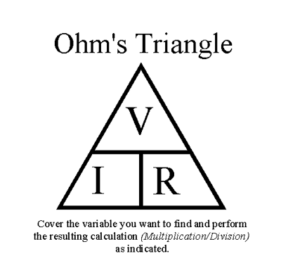
Figure 2.3 Ohm’s Law triangle
Let’s see how these equations might work to help us analyze simple circuits:
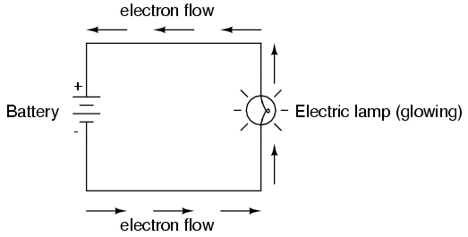
Figure 2.4 Electron flow
In the above circuit, there is only one source of voltage (the battery, on the left) and only one source of resistance to current (the lamp, on the right). This makes it very easy to apply Ohm’s Law. If we know the values of any two of the three quantities (voltage, current, and resistance) in this circuit, we can use Ohm’s Law to determine the third.
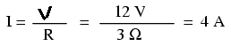
In this first example, we will calculate the amount of current (I) in a circuit, given values of voltage (V) and resistance ®:
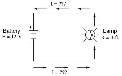
Figure 2.5 Ohms law problem 1
What is the amount of current (I) in this circuit?
Note the arrows showing the flow of electrons. Another very important point is established here. In a series circuit, that is a circuit where all the components are connected end to end, the current has the same numeric value wherever the circuit is broken to measure it. In other words, in the above example I = 4A, in the top and bottom connecting wires and even inside the battery and bulb if we could physically invade their space with a measuring instrument or ammeter!
In this second example, we will calculate the amount of resistance ® in a circuit, given values of voltage (V) and current (I):
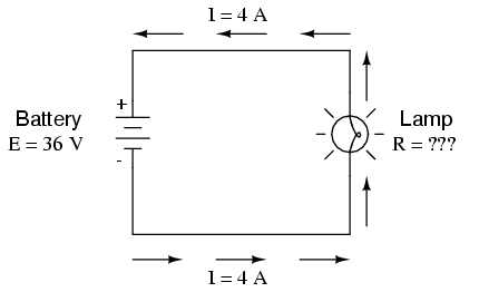
Figure 2.6 Ohms Law Problem 2
What is the amount of resistance R offered by the lamp?
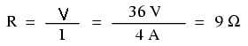
In the last example, we will calculate the amount of voltage supplied by a battery, given values of current (I) and resistance ®:
Figure 2.7 Ohms Law Problem 3
What is the amount of voltage provided by the battery?
![]()
Ohm’s Law is a very simple and useful tool for analyzing electric circuits. It is used so often in the study of electricity and electronics that it needs to be committed to memory by the serious student. For those who are not yet comfortable with algebra, then use the memory triangle!
REVIEW:
· Voltage measured in volts, symbolized by the letters ‘V’
· Current measured in amps, symbolized by the letter “I”.
· Resistance measured in ohms, symbolized by the letter “R”.
· Ohm’s Law: V = IR ; I = V/R ; R = V/I
An analogy for Ohm’s Law
Ohm’s Law also makes intuitive sense if you apply if to the water-and-pipe analogy. If we have a water pump that exerts pressure (voltage) to push water around a “circuit” (current) through a restriction (resistance), we can model how the three variables interrelate. If the resistance to water flow stays the same and the pump pressure increases, the flow rate must also increase.
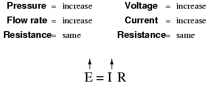
If the pressure stays the same and the resistance increases (making it more difficult for the water to flow), then the flow rate must decrease:
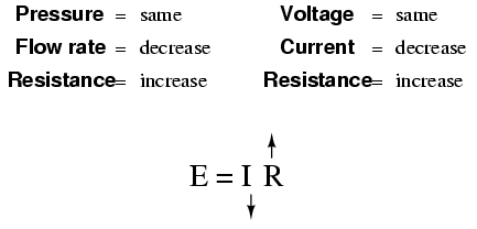
If the flow rate were to stay the same while the resistance to flow decreased, the required pressure from the pump would necessarily decrease:
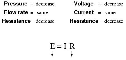
As odd as it may seem, the actual mathematical relationship between pressure, flow, and resistance is actually more complex for fluids like water than it is for electrons. If you pursue further studies in physics, you will discover this for yourself. Thankfully for the electronics student, the mathematics of Ohm’s Law is very straightforward and simple.
Graphical Representation of Ohms Law
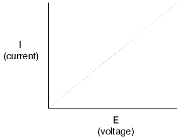
Figure 2.8 Graphical Ohm’s Law
The straight-line plot of current over voltage indicates that resistance is a stable, unchanging value for a wide range of circuit voltages and currents. In an “ideal” situation, this is the case. Resistors, which are manufactured to provide a definite, stable value of resistance, behave very much like the plot of values seen above. A mathematician would call their behavior “linear.”
This linear behavior shows us the graphical behavior of a resistor obeying Ohms Law.
Strictly speaking bulbs and lamps, although we have used them to illustrate some simple problems on Ohms Law are not very linear in resistance because their resistance changes as they got hot.
Figure 2.9 Diode symbol
DIODES
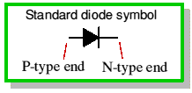 A diode,
literally meaning two electrodes, is a one way device with a non-linear current
–voltage characteristic. Unlike a
resistor, the amount of current through a diode will depend upon ‘which way
round’ we apply the voltage.
A diode,
literally meaning two electrodes, is a one way device with a non-linear current
–voltage characteristic. Unlike a
resistor, the amount of current through a diode will depend upon ‘which way
round’ we apply the voltage.
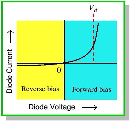
Figure 2.10
In figure 2.10 ,Vd is known as the diode turn on voltage it is usually about 0.6 -0.7 volts for a silicon diode. It is 0.2 volts for a germanium diode and even lower for metal-semiconductor or schottky barrier diodes. So didode turn on voltage depends on the semi-conductor marterial from which the diode is made.
REVIEW:
· With resistance steady, current follows voltage (an increase in voltage means an increase in current, and visa-versa).
· With voltage steady, changes in current and resistance are opposite (an increase in current means a decrease in resistance, and visa-verse).
· With current steady, voltage follows resistance (an increase in resistance means an increase in
· In resistors current voltage characteristic is linear.
· In hot bulbs it deviates from linear
· • In diodes it is so highly non-linear they act as one way devices.
CHAPTER 3: PRACTICAL RESISTORS
Because the relationship between voltage, current, and resistance in any circuit is so regular, we can reliably control any variable in a circuit simply by controlling the other two. Perhaps the easiest variable in any circuit to control is its resistance. This can be done by changing the material, size, and shape of its conductive components for instance; a thin metal filament of a lamp creates more electrical resistance than a thick wire.
Special components called resistors are made for the express purpose of creating a precise quantity of resistance for insertion into a circuit. They are typically constructed of metal wire or carbon, and engineered to maintain a stable resistance value over a wide range of environmental conditions. Unlike lamps, they do not produce light, but they do produce heat as electric power is dissipated by them in a working circuit. Typically, though, the purpose of a resistor is not to produce usable heat, but simply to provide a precise quantity of electrical resistance.
Resistors come in all sorts of values form fractions of an ohm up to 1000 Mega Ohms and with power ratings from typically 1/8th watt to tens or even hundreds of watts. Resistors come in three basic constructions been made either in wire wound found form using resistance wire usually on a ceramic or similar former the wire might be covered with a protective layer or alternatively they may be of carbon film or metal/metal oxide film construction. On wire wound types the value in ohms is often physically written on the body of the resistor. With other types a printed color code is used.
Colour codes
How can the value of a resistor be worked out from the colours of the bands? Each color represents a number according to the following scheme:
Figure 3.1 Resistor Color Codes
|
Number |
Color |
|
0 |
black |
|
1 |
brown |
|
2 |
red |
|
3 |
orange |
|
4 |
yellow |
|
5 |
green |
|
6 |
blue |
|
7 |
violet |
|
8 |
grey |
|
9 |
white |
|
|
|
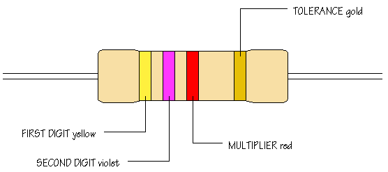
Figure 3.2 Colour code worked
example
For the resistor shown in figure
3.2, the first band is yellow, so the first digit is 4:The second band gives
the SECOND DIGIT. This is a violet band, making the second digit 7. The third
band is called the MULTIPLIER and is not interpreted in quite the same way. The
multiplier tells you how many noughts you should write after the digits you
already have. A red band tells you to add 2 noughts. The value of this resistor
is therefore 4 7 0 0 ohms, that is, 4 700 ![]() , or 4.7
, or 4.7 ![]() . Work through this example again to confirm
that you understand how to apply the colour code given by the first three
bands.
. Work through this example again to confirm
that you understand how to apply the colour code given by the first three
bands.
The remaining band is called the TOLERANCE band, see figure 3.3. This indicates the percentage accuracy of the resistor value. Most carbon film resistors have a gold-coloured tolerance band, indicating that the actual resistance value is with + or - 5% of the nominal value. Other tolerance colours are:
|
Tolerance |
Colour |
|
±1% |
brown |
|
±2% |
red |
|
±5% |
gold |
|
±10% |
silver |
Figure 3.3 Resistor Tolerances
When you want to read off a resistor value, look for the tolerance band, usually gold, and hold the resistor with the tolerance band at its right hand end. Reading resistor values quickly and accurately isn’t difficult, but it does take practice!
The actual tolerances of resistors readily available to purchase of the shelf depend on specific tolerance series known as E12 and E24.
E12 and E24 values
If you have any experience of
building circuits, you will have noticed that resistors commonly have values
such as 2.2 ![]() , 3.3
, 3.3 ![]() , or 4.7
, or 4.7 ![]() and are not available in equally spaced
values 2
and are not available in equally spaced
values 2 ![]() , 3
, 3 ![]() , 4
, 4 ![]() , 5
, 5 ![]() and so on. Manufacturers don’t produce values
like these - why not? The answer is partly to do with the fact that resistors
are manufactured to percentage accuracy. Look at the table below which
shows the values of the E12 and E24 series:
and so on. Manufacturers don’t produce values
like these - why not? The answer is partly to do with the fact that resistors
are manufactured to percentage accuracy. Look at the table below which
shows the values of the E12 and E24 series:
|
E12 series |
E24 series |
|
10 |
10 |
|
11 |
|
|
12 |
12 |
|
13 |
|
|
15 |
15 |
|
16 |
|
|
18 |
18 |
|
20 |
|
|
22 |
22 |
|
24 |
|
|
27 |
27 |
|
30 |
|
|
33 |
33 |
|
36 |
|
|
39 |
39 |
|
43 |
|
|
47 |
47 |
|
51 |
|
|
56 |
56 |
|
62 |
|
|
68 |
68 |
|
75 |
|
|
82 |
82 |
|
91 |
Figure 3.4 E12 AND E24 Series
Resistors are made in multiples of
these values, for example, 1.2 ![]() , 12
, 12 ![]() , 120
, 120 ![]() , 1.2
, 1.2 ![]() , 12
, 12 ![]() , 120
, 120 ![]() and so on.
and so on.
Consider 100 ![]() and 120
and 120 ![]() , adjacent values in the E12 range. 10% of
100
, adjacent values in the E12 range. 10% of
100 ![]() is 10
is 10 ![]() , while 10% of 120
, while 10% of 120 ![]() is 12
is 12 ![]() . A resistor marked as 100
. A resistor marked as 100 ![]() could have any value from 90
could have any value from 90 ![]() to 110
to 110 ![]() , while a resistor marked as 120
, while a resistor marked as 120 ![]() might have an actual resistance from 108
might have an actual resistance from 108 ![]() to 132
to 132 ![]() . The ranges of possible values overlap, but
only slightly.
. The ranges of possible values overlap, but
only slightly.
Further up the E12 range, a
resistor marked as 680 ![]() might have and actual resistance of up to
680+68=748
might have and actual resistance of up to
680+68=748 ![]() , while a resistor marked as 820
, while a resistor marked as 820 ![]() might have a resistance as low as 820-82=738
might have a resistance as low as 820-82=738 ![]() . Again, the ranges of possible values just
overlap.
. Again, the ranges of possible values just
overlap.
The E12 and E24 ranges are designed to cover the entire resistance range with the minimum overlap between values. This means that, when you replace one resistor with another marked as a higher value, its actual resistance is almost certain to be larger.
From a practical point of view, all that matters is for you to know that carbon film resistors are available in multiples of the E12 and E24 values. Very often, having calculated the resistance value you want for a particular application, you will need to choose the nearest value from the E12 or E24 range.
Some exam boards such as, for example AQA give all the colour codes and tolerances in their data sheets so you don’t always have to worry about learning this stuff and you only need to know about the E12 series.
Power rating
We have seen that as a consequence
of their action resistors dissipate heat
according to P=IV.
A resistor’s ability to lose heat depends to a large extent upon its surface area. A small resistor with a limited surface area cannot dissipate (=lose) heat quickly and is likely to overheat if large currents are passed. Larger resistors dissipate heat more effectively.
Look at the diagram below which shows resistors of different sizes:
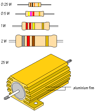
FIGURE 3.5 Resistor power rating actual physical sizes
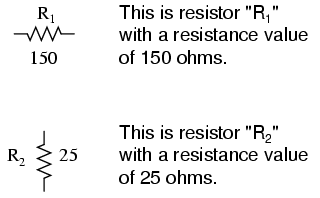
In keeping with their physical appearance the most common schematic symbol for a resistor is a small rectangular box, as seen previously. Sometimes, however, the zig zag symbol for a resistor is used
![]()
Resistor values in ohms are usually shown as an adjacent number, and if several resistors are present in a circuit, they will be labeled with a unique identifier number such as R1, R2, R3, etc. As you can see, resistor symbols can be shown either horizontally or vertically:
Real resistors look nothing like the zig-zag symbol. Instead, they look like small tubes or cylinders with two wires protruding for connection to a circuit. Here is a sample of some more different kinds and sizes of resistors:
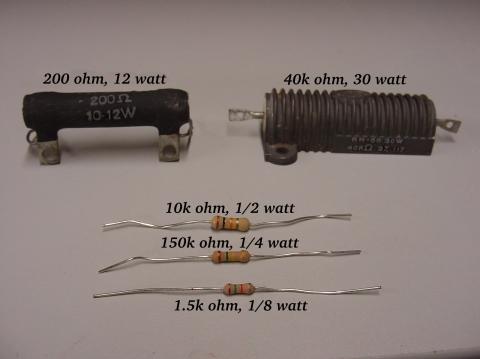
Figure 3.6 Selected wire wound and film resistors
Printed codes
Wire wound ceramic coated resistors so made for heat dissipation often have printed codes stamped on them.
High power
resistors get hot when used at the limit of their ratings and would quickly
discolour any
paint bands, so their values are printed on to them in number form. You
will not find
any decimal points on these markings, as they would easily be missed,
4.7kΩ is
written as 4K7, where the K stands for thousand Ohms, the unit not being
included
since all resistors are measured in Ohms.
The K is also
placed where the decimal point would have been. R is used instead of Ω
so 4R7 is
4.7Ω. M is used for millions of Ohms in the same way so 4M7 is
4,700,000Ω.
Tolerance is
also given by a letter code, J = 5%, and K = 10% are the two most
common.
Sometimes it is useful to create a variable resistor. These can have applications as resistive input transducers turning angular position into an output voltage or current.
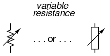
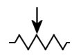
Variable resistor /potentiometer
Variable resistors must have some physical means of adjustment, either a rotating shaft or lever that can be moved to vary the amount of electrical resistance. Here is a photograph showing some devices called potentiometers, which can be used as variable resistors:
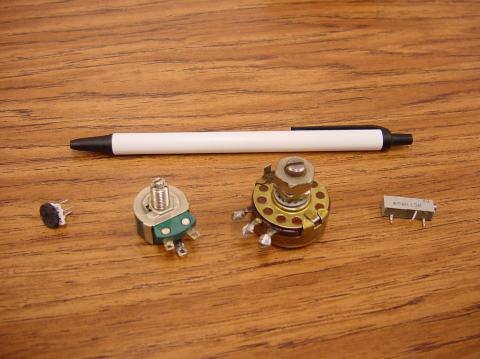
Figure 3.7 Selected variable resistors
Because resistors dissipate heat energy as the electric currents through them overcome the “friction” of their resistance, resistors are also rated in terms of how much heat energy they can dissipate without overheating and sustaining damage. Naturally, this power rating is specified in the physical unit of “watts.” Most resistors found in small electronic devices such as portable radios are rated at ¼ (0.25) watt or less. The power rating of any resistor is roughly proportional to its physical size. Note in the first resistor photograph how the power ratings relate with size: the bigger the resistor, the higher its power dissipation rating. Also note how resistances (in ohms) have nothing to do with size!
Although it may seem pointless now to have a device doing nothing but resisting electric current, resistors are extremely useful devices in circuits. Because they are simple and so commonly used throughout the world of electricity and electronics, we’ll spend some time analyzing circuits composed of nothing but resistors and batteries. A potentiometer as its name suggests is useful in dividing electric potential or voltage. If one connects the potentiometer across a battery then the voltage at the slider is determined simply by the ratio of the resistances in the two halves of the potentiometer.
For a practical illustration of resistors’ usefulness, examine the photograph below. It is a picture of a printed circuit board, or PCB: an assembly made of sandwiched layers of insulating phenolic fiber-board and conductive copper strips, into which components may be inserted and secured by a low-temperature welding process called “soldering.” The various components on this circuit board are identified by printed labels. Resistors are denoted by any label beginning with the letter “R”.
Figure
3.8 Modem PCB showing surface mount chip resistors and other components
This particular circuit board is a computer accessory called a “modem,” which allows digital information transfer over telephone lines. There are at least a dozen resistors (all rated at ¼ watt power dissipation) that can be seen on this modem’s board. Every one of the black rectangles (called “integrated circuits” or “chips”) contain their own array of resistors for their internal functions, as well.
Another circuit board example shows resistors packaged in even smaller units, called “surface mount devices.” This particular circuit board is the underside of a personal computer hard disk drive, and once again the resistors soldered onto it are designated with labels beginning with the letter “R”:
Figure 3.9 Computer floppy drive underside showing chip resistors
There are over one hundred surface-mount resistors on this circuit board, which is actually on the underside of a computer floppy disc drive and this count of course does not include the number of resistors internal to the black “chips.” These two photographs should convince anyone that resistors—devices that “merely” oppose the flow of electrons—are very important components in the realm of electronics!
In schematic diagrams, resistor symbols are sometimes used to illustrate any general type of device in a circuit doing something useful with electrical energy. Any non-specific electrical device is generally called a load, so if you see a circuit diagram showing a resistor symbol labeled “load,” especially in a tutorial circuit diagram explaining some concept unrelated to the actual use of electrical power, that symbol may just be a kind of shorthand representation of something else more practical than a resistor.
REVIEW:
· Devices called resistors are built to provide precise amounts of resistance in electric circuits. Resistors are rated both in terms of their resistance (ohms) and their ability to dissipate heat energy (watts).
· Resistor resistance ratings cannot be determined from the physical size of the resistor(s) in question, although approximate power ratings can.
CHAPTER FOUR:
MORE CIRCUITS AND RESISTOR CALCULATIONS
Circuit wiring
So far, we’ve been analyzing single-battery, single-resistor circuits with no regard for the connecting wires between the components, so long as a complete circuit is formed. Does the wire length or circuit “shape” matter to our calculations?
When we draw wires connecting points in a circuit, we usually assume those wires have negligible resistance. As such, they contribute no appreciable effect to the overall resistance of the circuit, and so the only resistance we have to contend with is the resistance in the components. Exceptions to this rule exist in power system wiring, where even very small amounts of conductor resistance can create significant voltage drops given normal (high) levels of current.
Knowing that electrically common points have zero voltage drops between them is a valuable troubleshooting principle. If I measure for voltage between points in a circuit that are supposed to be common to each other, I should read zero. If, however, I read substantial voltage between those two points, then I know with certainty that they cannot be directly connected together. If those points are supposed to be electrically common but they register otherwise, then I know that there is an “open failure” between those points. This will prove invaluable in diagnosing faults in any project circuits you might construct.
ESSENTIAL POINTS ON CIRCUIT WIRING:
· Connecting wires in a circuit are assumed to have zero resistance unless otherwise stated.
· Wires in a circuit can usually be shortened or lengthened without impacting the circuit’s function—all that matters is that the components are attached to one another in the same sequence. The exception to this is with circuits which conduct very high frequency alternating currents.
· Points directly connected together in a circuit by zero resistance (wire) are considered to be electrically common.
· Electrically common points, with zero resistance between them, will have zero voltage dropped between them, regardless of the magnitude of current (ideally).
· The voltage or resistance readings referenced between sets of electrically common points will be the same.
· These rules apply to ideal conditions, where connecting wires are assumed to possess absolutely zero resistance. In real life this will probably not be the case, but wire resistances should be low enough so that the general principles stated here still hold.
.
Resistors in series and potential dividers
As we have already seen for a series circuit, the current flowing is the same at all points. The circuit diagram below shows two resistors connected in series with a 6 V battery:
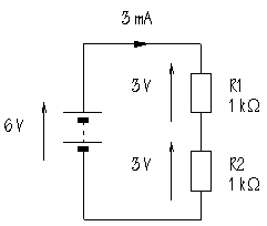 Figure
4.1.Resistors in series
Figure
4.1.Resistors in series
It doesn’t matter where in the circuit the current is measured; the result will be the same. The total resistance is given by:
|
|
In this circuit, Rtotal=
1+1= 2 ![]() . What will be the current flowing? The
formula is:
. What will be the current flowing? The
formula is:
|
|

Substituting:
Notice that the current value is
in mA when the resistor value is substituted in![]() .
.
The same current, 3 mA, flows through each of the two resistors. What is the voltage across R1? The formula is:
|
|
Substituting:
![]()
What will be the voltage across R2? This will also be 3 V. It is important to point out that the sum of the voltages across the two resistors is equal to the power supply voltage. In other word the two series resistors are acting a potential divider.
The essential circuit of a voltage divider, also called a potential divider, is:
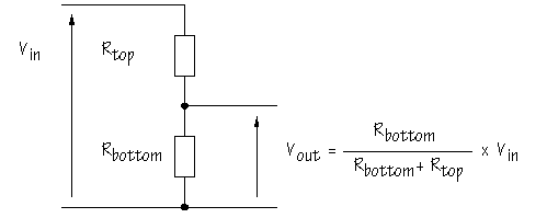
Figure 4.2 The potential divider
As you can see, two resistors are
connected in series. With Vin , which is often the power
supply voltage, connected above Rtop . It may help you to
remember that Rbottom appears on the top line of the
formula because Vout is measured across Rbottom
.
Some text books use labels R1 AND R2 for Rbottom and Rtop but unhelpfully some examination questions use R2 AND R1 OR even RA AND RB, hence the more unforgettable and less confusing method which has been adopted here.
Another way of thinking about a potential divider is to reference the negative pole of the battery to 0 volts and draw it at the bottom of the page. Then full maximum (positive) potential will be at the top of the diagram and you can think of climbing up the potential ladder of the resistors rather as counting up rungs of a number ladder.
Potential divider circuits have important applications in sensor input sub-systems for example when used with LDR’S (Light dependent Resistors) to form light sensors or when used with Thermistors (see later) to form temperature sensors.
Resistors in parallel
The next circuit shows two resistors connected in parallel to a 6 V battery:
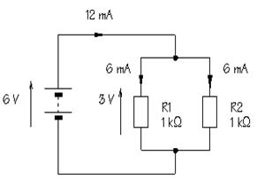 Figure 4.3 Resistors in parallel
Parallel circuits always provide alternative pathways for current flow. Note the resistors are drawn side to side in the diagram not end to end as was the case in the series circuit. The total resistance for the parallel circuit is calculated from:
|
|
This is called the product over sum formula and works for any two resistors in parallel. An alternative more general formula is:
|
|
This formula can be extended to work for more than two resistors in parallel, but lends itself less easily to mental arithmetic. Both formulae are correct.
What is the total resistance in this circuit?
The current can be calculated from:
How does this current compare with the current for the series circuit? It’s more. This is sensible. Connecting resistors in parallel provides alternative pathways and makes it easier for current to flow. How much current flows through each resistor? Because they have equal values, the current divides, with 6 mA flowing through R1, and 6 mA through R2.
To complete the picture, the voltage across R1 can be calculated as:
![]()
This is the same as the power supply voltage. The top end of R1 is connected to the positive terminal of the battery, while the bottom end of R1 is connected to the negative terminal of the battery. With no other components in the way, it follows that the voltage across R1 must be 6 V. What is the voltage across R2? By the same reasoning, this is also 6 V.
|
ESSENTIAL POINT: |
When components are connected in parallel, the voltage across them is the same. |
Here is a slightly more complex circuit, with both series and parallel parts:
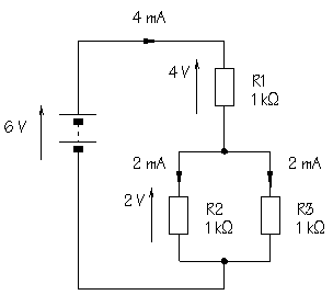
Figure 4.4 Circuit with series and parallel resistors
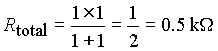
To find the overall resistance,
the first step is to calculate the resistance of the parallel elements. You
already know that the combined resistance of two 1 ![]() resistors in parallel is 0.5
resistors in parallel is 0.5 ![]() , so the total resistance in the circuit is
1+0.5 = 1.5
, so the total resistance in the circuit is
1+0.5 = 1.5 ![]() . The power supply current is:
. The power supply current is:
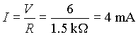
This is the current which flows through R1. How much current will flow through R2? Since there are two equally easy pathways, 2 mA will flow through R2, and 2 mA through R3.
The voltage across R1 is given by:
![]()
This leaves 2 V across R2 and R3, as confirmed by the calculation for R2:
![]()
Again, the sum of the voltages around the circuit is equal to the power supply voltage.
Check through this section carefully. A clear understanding of the concepts involved will help tremendously.
CHAPTER 5: SYSTEMS AND
SUB-SYSTEMS
Although from what you have
read so far you will now have some
understanding of how very basic electronic components work, it is often easier
to make sense of whole electronic circuits as systems in terms of their over
all purpose and structure or major chunks thereof (sub-systems). Indeed this
approach has radically changed the study and practice of electronics has
changed in recent years.
Previously, electronic
circuits were designed by looking at the behaviour of all their individual
components such as resistors, capacitors and transistors.
Electronics designers
have found that there are fairly standard ways of assembling components which
allowed them to produce ‘building blocks’ or ‘system blocks’. In fact as such Engineers
have a way of showing the functionality of Electronic gismos without
necessarily showing all the complexity. This can be done by the use of what is
referred to as a System Diagram sometimes the word Block is inserted in place of the
word System.
Using these building
blocks it is possible to choose particular combinations which allow you to
build almost any circuit you could wish to.
This is known as a systems approach to electronics. The building blocks are known as subsystems. Those of you who do Computer Studies may have come across a similar concept in Flow Diagrams, which also incidentally comprises part of the A2 content of this book.
All known subsystems can
be divided into one of four categories:
A systems diagram in its
simplest form consists of just these three basic elements. You must remember
that a power supply will always be present even though it is rarely shown in a
systems diagram and a Driver is often required between the Process
and Output stages.
Below Figure 5.1 Systems and
sub-systems
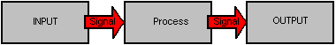
The arrows connecting
the subsystems together show the direction of the energy or information flow.
This energy which carries the information is in the form of an electrical
signal. The different kinds of signal are looked at later.
Input subsystems usually
convert information from the outside world into electrical energy. A few,
however, generate a signal independently.
Input subsystems: take
information about the outside world from sensors and convert it into an
electronic signal which is passed to the next subsystem (usually a
process subsystem such as a Comparator or an Amplifier or a Logic stage). This
is not true of all input subsystems however because some of them generate their
own signal. Two of these are shown below:
Pulse
Unit: Generates on/off pulses. Adjust the dial to vary the pulse rate
Voltage
reference: generates a very steady
Signal
generator /oscillator : generates sine waves and other
time varying signals.
Neither must we forget that each and every sub-system needs powering up by a battery or a power supply in order to its job, but these are rarely if ever shown in system diagrams.
The desk top P.C and its typical input devices can be classically represented by a system diagram:
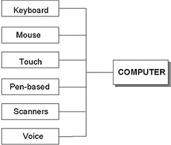
Figure 5.2 The desk top P.C. as a system diagram
The precise circuitry content of each subsystem depends on the job in hand which the system needs to perform. Take a simple darkness sensor for instance. The input subsystem might contain an LDR (Light dependent resistor) in a potential divider network with a resistor. The processing subsystem might a circuit to determine what light level (voltage output from divider) to turn on a lamp. Finally the output subsystem might contain a lamp or a circuit to drive the lamp and a lamp.
We now have a good idea about what an electronic system know as a darkness sensor does, without precise knowledge of the circuit detail within. Thus system diagrams a very good for conveying a basic idea of how something works, or for that matter, the elements or building blocks required to make something work, or perform a particular function, without worrying too much about the detail.
When all is said and done there is really no such thing as a new or novel electronic circuit. The fundamental building blocks of electronics have remained unchanged for some time now. However, there may be novel ways of stitching these building blocks tighter to solve fundamental, everyday, problems electronically. This forms a fundamental part of much GCSE and A-level coursework.
Using
a systems approach
Simple
changes to one sub-system can bring about a huge change in the operation of the
system as whole. Take our darkness sensor, for example. If we
change one component in the input sub-system say from an LDR to a Thermistor
then our whole System would become a low
–temperature indicator! If we used
a microphone in our input sub-system with an appropriate amplifier, our whole
system would become a Sound to light converter!
Sensors are input subsystems that monitor
changes in the environment. Inverting a Sensor subsystem reverses its
operation. For example, a light sensor would become a dark sensor!
REVIEW
· System Diagrams are a way of showing the functionality of Electronic gismos without necessarily showing all the complexity.
· The simplest System Diagram has just three sub-systems; input, process and output.
· Simply changing a part of one sub-system can fundamentally change the purpose of the system as a whole.
CHAPTER 6: RESITIVE INPUT
DEVICES, SENSORS AND SUB-SYSTEMS.
Some typical input sub-systems which may find themselves integrated into a resistive potential divider circuit during use are listed in the table below :
|
|
Light
Sensor: ( LDR) Measures the amount
of light. |
|
|
Moisture
Sensor: Measures the moisture level. |
|
|
Push
Switch: Provides an intermittent ‘on’ switch. |
|
|
Reed
Switch: Provides a switch that operates when a magnet is brought
near. |
|
|
Rotation
Sensor: Measures rotation. |
|
|
Sound
Sensor: Measures the sound level. |
|
|
Temperature
Sensor: (often Thermistor) Measures the temperature. |
|
|
Tilt
Switch: Provides a switch that operates when tilted. |
The input transducers
described in this section and the associated calculations are key exam topics.
LDRS
Let us examine in more detail the
Components and circuit detail required for a light (or darkness) sensor input
subsystem. The main component is a specialist resistor known as an LDR or Light
Dependent Resistor. The device contains
the semiconductor material Cadmium Sulfide and in some countries and texts may referred
to as a CDS or CDS Sensor. 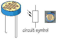
Figure 6.1 Light Dependent Resistors
An LDR is an input transducer (sensor) which converts brightness (light) to resistance. It has a resistance which decreases as the brightness of light falling on the LDR increases.
A multimeter can be used to find the resistance in darkness and bright light, these are the typical results for a standard LDR:
·
Darkness: maximum resistance, about 1M![]() .
.
·
Very bright light: minimum resistance, about 100![]() .
.
For many years the standard LDR has been the ORP12, now the NORPS12, which is about 13mm diameter. Miniature LDRs are also available and their diameter is about 5mm.
An LDR may be connected either way
round and no special precautions are required when soldering. A practical investigation of an LDR may be
made as follows using a breadboard , a fixed resistor , a 9volt battery and a
multimeter.
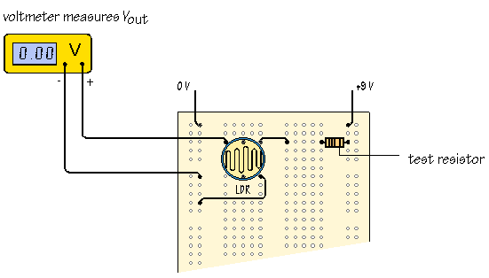
Figure 6.2 Measurement of LDR characteristic
If you set this up, you will be
able to verify the behavior of the LDR in response to various light
levels. 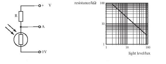
Figure 6.3 LDR circuit arrangement Figure 6.4 LDR characteristic
Your experiment will convince you that in a practical input sub-system, one of the resistors in a voltage divider is replaced by an LDR. You may obtain a graph rather like the one above. It is called a LOG- LOG plot.
In the circuit below, Rtop
is a 10 ![]() resistor, and an LDR is used as Rbottom
:
resistor, and an LDR is used as Rbottom
:
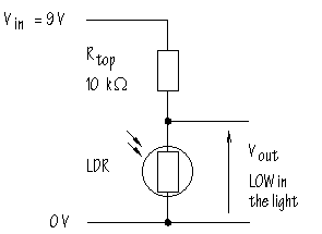
Figure 6.5 Dark sensor
Suppose the LDR has a resistance
of 500 ![]() , 0.5
, 0.5 ![]() , in bright light, and 200
, in bright light, and 200 ![]() in the shade (these values are reasonable).
in the shade (these values are reasonable).
When the LDR is in the light, Vout will be:
|
|
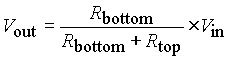
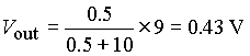
In the shade, Vout will be:
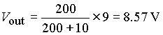
In other words, this circuit gives a LOW voltage when the LDR is in the light and a HIGH voltage when the LDR is in the shade. The voltage divider circuit gives an output voltage which changes with illumination.
A sensor subsystem which functions like this could be thought of as a ‘dark sensor’ and could be used to control lighting circuits which are switched on automatically in the evening. The HIGH voltage out is useful for driving LOGIC systems which we will meet later,
.
Here is the voltage divider built with the LDR in place of Rtop :
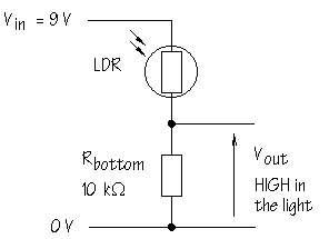
Figure 6. 6 Light sensor
What effect does this have on Vout ?
The action of the circuit is reversed. that is, Vout becomes HIGH when the LDR is in the light, and LOW when the LDR is in the shade. Substitute the appropriate values in the voltage divider formula to convince yourself that this is true.
You will realize that an LDR positioned hence in a potential divider can be used as a LIGHT SENSOR rather than a darkness sensor.
.
Temperature sensors
Replacing the LDR or light sensor with a temperature sensor would make an input sub-system with a very different function. Strangely, fundamentally the same resistive potential divider arrangement is used when using the common temperature sensor based on a temperature-sensitive resistor and called a thermistor. There are several different types:
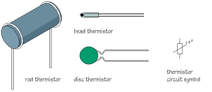
Figure 6.7 Various thermistors
The resistance of most common types of thermistor decreases as the temperature rises. They are called negative temperature coefficient, or ntc, thermistors. Note the -t° next to the circuit symbol. A typical ntc thermistor is made using semiconductor metal oxide materials. (Semiconductors have resistance properties midway between those of conductors and insulators.) As the temperature rises, more charge carriers become available and the resistance falls.
Although less often used, it is possible to manufacture positive temperature coefficient, or ptc, thermistors. These are made of different materials and show an increase in resistance with temperature.
How could you make a sensor circuit for use in a fire alarm? You want a circuit which will deliver a HIGH voltage when hot conditions are detected. You need a voltage divider with the ntc thermistor in the Rtop position:
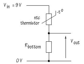 Figure 6.8 ‘Hot’ sensor
How could you make a sensor circuit to detect temperatures less than 4°C to warn motorists that there may be ice on the road? You want a circuit which will give a HIGH voltage in cold conditions. You need a voltage divider with the thermistor in place of Rbottom :
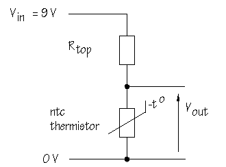 Figure 6.9 ‘Cold’ sensor
This last application raises an important question: How do you know what value of Vout you are going to get at 4°C?
To answer this question, you need to estimate the resistance of the thermistor at 4°C.
Lots of different types of
thermistor are manufactured and each has its own characteristic pattern of
resistance change with temperature. The diagram below shows the thermistor
characteristic curve for one particular thermistor:
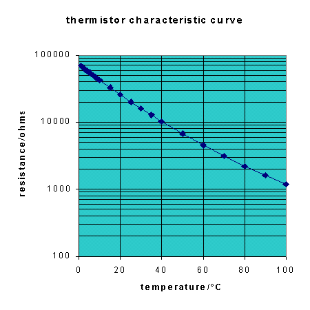
Figure 6.10 Thermistor
characteristic
On the y-axis, resistance is
plotted on a logarithmic scale. This is a way of compressing the graph so that
it is easier to see how the resistance changes. Between 100 ![]() and 1000
and 1000 ![]() , each horizontal division corresponds to 100
, each horizontal division corresponds to 100
![]() . On the other hand, between 1000
. On the other hand, between 1000 ![]() and 10000
and 10000 ![]() , each division corresponds to 1000
, each division corresponds to 1000 ![]() . Above 10000
. Above 10000 ![]() , each division respresents 10000
, each division respresents 10000 ![]() .
.
As you can see, this thermistor
has a resistance which varies from around 70 ![]() at 0°C to about 1
at 0°C to about 1 ![]() at 100°C. Suppliers catalogues usually give
the resistance at 25°C, which was 20
at 100°C. Suppliers catalogues usually give
the resistance at 25°C, which was 20 ![]() in this case. Usually, catalogues also
specify a ‘Beta’ or ‘B-value’. When these two numbers are specified, it is
possible to calculate an approximate value for the resistance of the thermistor
at any particular temperature from the equation:
in this case. Usually, catalogues also
specify a ‘Beta’ or ‘B-value’. When these two numbers are specified, it is
possible to calculate an approximate value for the resistance of the thermistor
at any particular temperature from the equation:
|
|
Where:
RT is the resistance at temperature T in Kelvin (= °C +273)
RT0 is the resistance at a reference
temperature T0 in Kelvin. When the reference
temperature is 25°C, T0 = 25+273. e is
the natural logarithm base, raised to the power ![]() in this equation.B
is the B-value specified for this thermistor.
in this equation.B
is the B-value specified for this thermistor.
You don’t need to think about
applying this equation at the moment, but it is useful to know that the
information provided in catalogues is sufficient to allow you to predict
thermistor performance. With RT0 = 20 ![]() and B =4200, resistance changes from
0 to 10°C are as follows:
and B =4200, resistance changes from
0 to 10°C are as follows:
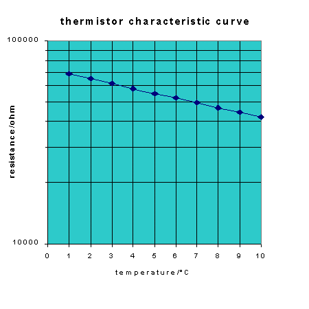
Figure 6.11 Thermistor
characteristic 0-10C
From the graph, the resistance at 4°C can be estimated as just a little less
than 60 ![]() . By calculation using the equation, the
exact value is 58.2
. By calculation using the equation, the
exact value is 58.2 ![]() . In the A-level examination you will most
likely only have to estimate thermistor values from a given graph. Precise
calculation will not be required.
. In the A-level examination you will most
likely only have to estimate thermistor values from a given graph. Precise
calculation will not be required.
|
KEY POINT: |
The biggest change in Vout from a voltage divider is obtained when Rtop and Rbottom are EQUAL in value. |
What this means is that selecting
a value for Rtop close to 58.2 ![]() will make the voltage divider for the ice
alert most sensitive at 4°C. The nearest E12/E24 value is 56
will make the voltage divider for the ice
alert most sensitive at 4°C. The nearest E12/E24 value is 56 ![]() . This matters because large changes in Vout
make it easier to design the other subsystems in the ice alert, so that
temperatures below 4°C will be reliably detected.
. This matters because large changes in Vout
make it easier to design the other subsystems in the ice alert, so that
temperatures below 4°C will be reliably detected.
Sensor devices vary considerably in resistance and you can apply this rule to make sure that the voltage dividers you build will always be as sensitive as possible at the critical point.
Thermistors turn up in more places than you might imagine. They are extensively used in cars, for example in:
· electronic fuel injection, in which air-inlet, air/fuel mixture and cooling water temperatures are monitored to help determine the fuel concentration for optimum injection.
· air conditioning and seat temperature controls.
· warning indicators such as oil and fluid temperatures, oil level and turbo-charger switch off.
· fan motor control, based on cooling water temperature
· frost sensors, for outside temperature measurement
· acoustic systems
· to measure air flow, for instance in monitoring breathing in premature babies.
Rotary Potentiometer as an Angle Sensor
In industrial electronics potentiometers are often used as angle and position sensors.
A typical input subsystem for this purpose is shown below:
Figure 6.12 Angle
Sensor
|
This block uses a potentiometer or variable resistor
as an angle sensor. If you wanted, you could attach a large knob or
disc to the potentiometer marked in degrees. Or you could use it to
measure the position of something else using a gear wheel or pulley.
The 1k resistor is just for protection in case the output gets shorted but is
not really necessary. |
|
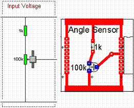
The output voltage at the slider will be directly proportional to the angle the slider is turned or rotated through if the potentiometer has good linearity.
Sound sensors
Another name for a sound sensor is a microphone. The diagram shows a cermet microphone:
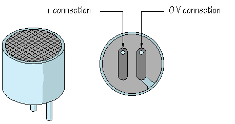
Figure 6.13 Cermet (Electret ) microphone
Cermet’ stands for ‘ceramic’ and ‘metal’. A mixture of these materials is used in making the sound-sensitive part of the microphone. To make them work properly, cermet microphones need a polarizing voltage, usually around 1.5 V across them. A suitable circuit for use with a 9 V supply is:
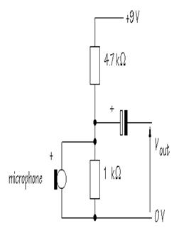
Figure 6.14 Microphone input
circuit
The 4.7 ![]() and 1
and 1 ![]() resistors make a voltage divider which
provides 1.6 V across the microphone. Sound waves generate small A.C. or
time varying changes in voltage, usually in the range 10-20 mV. To isolate
these small signals from the steady 1.6 V, a capacitor is
used. Capacitors are described later but basically can either be used as D.C.
blocking components or in timing circuits.
resistors make a voltage divider which
provides 1.6 V across the microphone. Sound waves generate small A.C. or
time varying changes in voltage, usually in the range 10-20 mV. To isolate
these small signals from the steady 1.6 V, a capacitor is
used. Capacitors are described later but basically can either be used as D.C.
blocking components or in timing circuits.
Signals from switches
When a switch is used to provide an input to a circuit, pressing the switch usually generates a voltage signal. It is the voltage signal which triggers the circuit into action. What do you need to get the switch to generate a voltage signal? . . . You need a voltage divider. The circuit can be built in either of two ways:
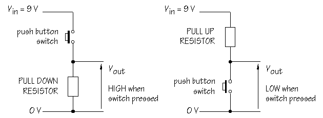
Figure 6.15 Logic signals from switches
The pull down resistor
in the first circuit forces Vout to become LOW except when
the push button switch is operated. This circuit delivers a HIGH voltage when
the switch is pressed. A resistor value of 10 ![]() is often used.
is often used.
In the second circuit, the pull up resistor forces Vout to become HIGH except when the switch is operated. Pressing the switch connects Vout directly to 0 V. In other words, this circuit delivers a LOW voltage when the switch is pressed.
In circuits which process logic signals, a LOW voltage is called ‘logic 0’ or just ‘0’, while a HIGH voltage is called ‘logic1’ or ‘1’. These voltage divider circuits are perfect for providing input signals for logic systems.
CHAPTER SEVEN:
INTRODUCTION TO LOGIC
DEVICES AND CIRCUITS; A SPECIAL CLASS OF PROCESS SUB-SYSTEMS.
Imagine we have a sensor whose output goes to zero or a very low voltage when it is activated. We could imagine this might be a tripwire for a burglar. Zero volts cannot directly activate an alarm so we might want to find some way of converting this zero or LOW (conveniently called Logic O in a Logic system) into a high voltage, say nearer the positive terminal voltage of the battery. The Logic component or sub-system to do this is called an Inventor Gate or more commonly a NOT gate. Our logic gate would be changing then the signal from an input sub-system so as such could be regarded as a special class of process sub-system.
In the electronics we have met so
far we have considered a full range of voltage levels from 0 to the battery
terminal voltage. This range is
continuous and called analogue.
Rather like switches, the operation of Logic gates only uses two discrete voltage levels, fully off or O and fully ON, or full supply voltage which in Logic terms we call LOGIC 1 . Logic gates therefore with only two possible states are said to work according to the Binary System of Arithmetic. In fact for Electronics training purposes Logic gates are often represented by combinations of switches or relays (special electromagnetic switches which we shall meet later). However in practice logic gates contain solid state components (that is with no moving parts) and are implemented using various types of transistors and diodes or metal oxide semiconductor devices.
The behavior of Logic Gates can be described to some extent by their symbols but more accurately by their Truth Tables or Boolean expressions. Boolean expressions are a feature of Boolean algebra a special type of Arithmetic relevant to Logic gates and Logic Systems.
NOT GATE TRUTH TABLE 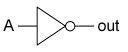 Figure 7.1 NOT gate symbol
|
INPUT |
OUTPUT Q |
|
A |
NOT A |
|
0 |
1 |
|
1 |
0 |
Figure 7.2 NOT gate truth table
Not Gate Boolean Algebra:
_
Q = A
(The
bar over the top means the opposite of the logic level of A.)
It reads ‘Q = A bar’.
AND GATES
Let us consider another problem. Imagine we want to make a very simple burglar alarm. We have an ‘arming’ switch for the alarm and a door sensor both giving high voltage outputs (LOGIC 1’S). We do not want the alarm to go off during the day when we are opening and closing the day if we are in, so the arming switch is in the off (LOGIC 0) position. At night when the alarm is armed, the condition of someone forcing the door needs to set off the alarm. In other words ‘arming’ AND ‘door forcing’ both need to give LOGIC 1 signals at an output together to set to set off the alarm. The logic gate or sub-system to bring about this effect is called an AND gate.
|
Type |
Distinctive shape |
Rectangular shape |
|
AND |
|
|
|
|
Like a letter D in AND |
|

Figure 7.3 AND GATE Symbol
Figure 7.4 AND GATE Truth Table
|
INPUT |
OUTPUT Q |
|
|
A |
B |
A AND B |
|
0 |
0 |
0 |
|
1 |
0 |
0 |
|
0 |
1 |
0 |
|
1 |
1 |
1 |
 Figure 7.5 AND gate switch
In figure 7.5, the switch circuit diagram for AND
gate, comprising two normally open ‘push’ swithces in series. The left hand connection goes to a battery or
power supply positive terminal.
Boolean Algebra: This is a way of writing an equation to represent an AND gate.
Q = A . B
We borrow the dot from conventional algebra due to the similarity
between multiplication and the AND process.
The table above could be a multiplication table for A × B, but it is
important to remember that Q = A AND B
is what is being represented here.
Switch circuit diagrams may help some students understand logic gates.
To do this you need think of the input action as being applied to the switches. A firm press is made to the switch corresponding to an INPUT at that letter, whereas no press is like LOGIC 0. Just remember with real logic gates the press at the input is given by a voltage usually +5 or sometimes +15 not by someone’s finger! Relays are electromagnetic switches that can be activated by voltage in this way and in days gone by were actually used to implement logic!
Consider a third situation. We want a burglar alarm which will alarm if a burglar forces EITHER a door OR a window OR BOTH (It could even cope with two burglars at once!). Both our door and window sensors both give LOGIC 1 when forced. The logic gate to do this job is called an OR gate.
|
OR |
|
|

Figure 7.6
Note the distinctive shape of the OR GATE SYMBOL in figure 7.6. A good memory aid is to think of the word AR(RO)W which contains OR and describes the arrow head shape!
Figure 7.7 The truth table of an OR gate
|
INPUT |
OUTPUT Q |
|
|
A |
B |
A OR B |
|
0 |
0 |
0 |
|
1 |
0 |
1 |
|
0 |
1 |
1 |
|
1 |
1 |
1 |
Boolean
algebra:
Q = A
+ B

Figure 7.8 Switch circuit diagram for OR gate
Four other types of Logic gate are also available. Try to dream up sensor or alarm situation input situations where these might be useful yourselves. The first of these is the NAND gate NAND standing for NOT AND, it is rather like having an AND gate with a NOT gate connected to its output.
NAND
![]()
Note shape is like AND but with a small negation circle or ‘bubble’ on the output.
That is, the output is 1 when NOT (A AND B are 1), as shown in the truth table.
 Figure 7.9 Switch circuit of NAND gate
|
INPUT |
OUTPUT |
|
|
A |
B |
A NAND B |
|
0 |
0 |
1 |
|
1 |
0 |
1 |
|
0 |
1 |
1 |
|
1 |
1 |
0 |
Figure 7.10 Truth Table NAND GATE
Switch circuit diagram of NAND gate. Note this time normally closed push
swithces are used.
Note how the truth table outputs are the opposites (NOTS) of the AND GATE
TABLE.
Boolean algebra:
____
Q = A . B
(Q equals A AND B all bar.)
NOR GATE
Similarly, the NOR gate is the NOT of an OR gate. That is, the output is 1
only when both inputs are 0, as shown in the truth table.
|
INPUT |
OUTPUT Q |
|
|
A |
B |
A NOR B |
|
0 |
0 |
1 |
|
1 |
0 |
0 |
|
0 |
1 |
0 |
|
1 |
1 |
0 |

Figure 7.11 Switch circuit
diagram of NOR gate
Figure 7.12 Truth Table NOR
gate
Boolean algebra:
_____
Q = A + B
(Q equals A OR B all bar.)
We say ‘all bar’ when the bar is over the whole term.
XOR and XNOR gates
These are the only other logic gates we will meet - XOR
(exclusive-OR) and XNOR (exclusive-NOR).
|
INPUT |
OUTPUT Q |
|
|
A |
B |
A XOR B |
|
0 |
0 |
0 |
|
0 |
1 |
1 |
|
1 |
0 |
1 |
|
1 |
1 |
0 |
The XOR is a ‘stricter’ version of the OR gate. Rather than all owing the output to be 1 when either one or both
of the inputs are 1, an XOR gate has a 1 output only when only one input
is 1. Thus, it has the truth table shown to the right. This can also be
interpreted (for a two-input gate) as “Output= LOGIC 1 , when the inputs are
different”.
Figure 7.13 Truth Table XOR
XOR Boolean Algebra:
Q = A Å B
(Q equals A EXOR B.)
XNOR GATE
|
INPUT |
OUTPUT Q |
|
|
A |
B |
A XNOR B |
|
0 |
0 |
1 |
|
1 |
0 |
0 |
|
0 |
1 |
0 |
|
1 |
1 |
1 |
XNOR is an inverted version of the XOR gate. Thus, it has the truth table
shown to the right. This can also be interpreted as
“ Output =Logic 1 when the inputs are same”. Its other name is the PARITY GATE because it outputs 1 when
inputs come in equal pairs.
Figure 7.14 Truth Table XNOR
Boolean algebra:
_____
Q = A Å B
(Q
equals A EXNOR B.)
The simple logic gates above can also be combined to form more complicated
Boolean logic circuits. Logic circuits are often classified in two groups: combinatorial logic, in which the outputs
are instant continuous-time functions of combinations at the inputs, and sequential
logic, in which the outputs depend on information stored by the
circuits as well as on the inputs and information may move fast or more slowly
in a step-wise manner through the system. We will meet Combinatorial Logic later
in this Chapter.
Some aspects of sequential logic will be dealt with elsehwere in the
book.
An alternative summary of the ‘electronic’ action of the common logic
families can be seen in the table, FIGURE 7.15.
|
OR |
Any high input will drive the output high |
|
NOR |
Any high input will drive the output low |
|
AND |
Any low input will drive the output low |
|
NAND |
Any low input will drive the output high |
|
|
Figure 7.15 LOGIC SUMMARY TABLE |
Introduction to Combinatorial Logic: Making Gates from NAND gates
It is more economical in cost, power consumption and space to make circuits from just one kind of chip since logic chips contain 4 or 6 logic gates and many circuits are made up of just NAND gates. Let us look how:
 Figure 7.16 NAND gate
The two inputs of a NAND gate connected together make the NAND gate into a NOT gate, see figure 7.16
In figure 7.17 the output of a NAND gate is inverted by the NOT gate to produce the output of an AND gate.
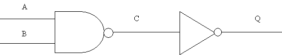
Figure 7.17 NAND and NOT
in series
Figure 7.18
NAND/NOT Combination Truth Table
|
A |
B |
C |
Q |
|
0 |
0 |
1 |
0 |
|
0 |
1 |
1 |
0 |
|
1 |
0 |
1 |
0 |
|
1 |
1 |
0 |
1 |
Now look at the circuit in figure 7.19
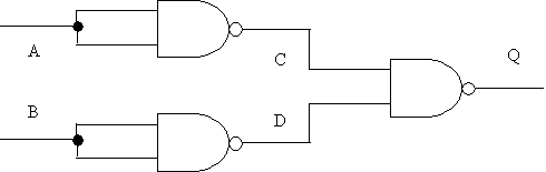
Figure 7.19 Three NAND
CIRCUIT
By working through logically and finding what the intermediate outputs C and D are,
you should be able to solve for Q.
Try working the
other way round; look at the truth table in figure 7.20.
|
|||||||||||||||||||||||||||||||
|
Two NAND gates used to simulate the AND gate. The truth table shows
how this happens the second NAND gate acts as an inverter because one input is held at logic 1 |
|
||||||||||||||||||||||||||||||
Figure 7.20 Two NAND Truth Table
Now try to draw the logic diagram. It is important you master this, you will be tested on these concepts in you’re a level exam. You will notice that there are two ways to make a NAND gate act as an Inverter .One is as in this example by holding one of its inputs at Logic 1. This can be done by connecting it directly to the +ve supply rail. The second way is by connecting both inputs of the NAND GATE together.
Introduction to Boolean algebra
Boolean algebra does the same job as a truth table, but is briefer to use and has symbols. A Boolean expression tells us what condition will give an output of 1.
In Boolean
algebra it is traditional but not essential to refer to the output logic level
of a gate as a capital letter Q.
For our NOT gate
the Boolean expression is:
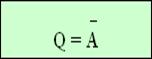 Figure 7.21 NOT Boolean
The symbol Ā is pronounced “A-bar”, and means that the state Q is opposite to the state Q. So the statement says “Q is equal to NOT A”. This means that the output Q is logic 1 when A is logic 0.
Remember if you are not sure of this you can check the NOT truth table in figure 7.2.
AND GATE BOOLEAN
For an AND gate the Boolean expression is:
![]() Figure 7.22 AND Boolean
Figure 7.22 AND Boolean
The dot between the A and the B mean that both A AND B have to be 1 for Q to be 1. The expression is pronounced, “Q equals A dot B”. Remember the equivalent truth table is:
|
A |
B |
Q |
|
0 |
0 |
0 |
|
1 |
0 |
0 |
|
0 |
1 |
0 |
|
1 |
1 |
1 |
For the
OR gate the Boolean expression is:
![]() Figure 7.23 OR Boolean
Figure 7.23 OR Boolean
This is pronounced, “Q is equal to A OR B” and remember the truth table is:
|
A |
B |
Q |
|
0 |
0 |
0 |
|
1 |
0 |
1 |
|
0 |
1 |
1 |
|
1 |
1 |
1 |
Practical Logic Gates
Perhaps the most common family of
Logic Gates in use by Electronics Engineers today is the 7400 series of TTL I.C.’S (transistor/transistor logic integrated
circuits). This family of logic operates from a +5
 Figure 7.24 Logic gate 14 Pin DIL
The example shown above is the SN 7400N quad NAND gate. Such packages are known as 14 pin D.I.L (as you can see there are two pairs of seven pins in a parallel line).
You will not be asked to recall manufactures I.C. numbering systems or pin connection numbers in any A-level examination. It is necessary however to be able to use manufacturers’ catalogues and data sheets for practical and project work. Note how pin1 of the I.C. is always located BELOW the left of the edge dimple when looking down on the chip from above. In some I.C.S it is also marked with a brown or black spot.
Although we have said that logic 0 is equivalent to 0volts and logic 1 to a high voltage or full supply voltage, different families of logic chips interpret practical voltages in different ways. Besides TTL logic it is possible you may also meet CMOS. The table shows how the two different families interpret voltages at their INPUT terminals:
|
Technology |
L voltage Logic 0 |
H voltage Logic 1 |
Notes |
|
0V to VCC/2 |
VCC/2 to VCC |
VCC = supply voltage Usually 5-15 volt. |
|
|
0V to 0.8V |
2V to VCC |
VCC is 4.75V to 5.25V |
Figure 7.25 Table of CMOS and TTL operating voltages
Common Basic Logic ICs
|
CMOS |
TTL |
Function |
|
Quad two-input NOR gate |
||
|
Quad two-input NAND gate |
||
|
Hex NOT gate (inverting buffer) |
||
|
Quad two-Input XOR gate |
||
|
Quad two-input OR gate |
||
|
Quad two-input XNOR gate |
||
|
Quad two-input AND gate |
||
|
|
|
Figure 7.26 |
CMOS logic ICs, including gates with more than two inputs, are described in
maufacturers’ catalogues as 4000 series.
You may
find the table above very useful if you are contemeplating using Logic I.C.’S
in your Course work. Although only two input gates have been dealt with here it
is possible to get gates with more inputs for instance 3 and 4 input AND and OR gates are quite common. You might be able
to relaise they would be useful in a more sophistaicated burglar alram with
multiple input sensors. The exception is of course the NOT gate which only ever has
one input!
REVIEW
·
Logic operates with only 2 states or
levels, known as Binary. Logic 0 =
0volts, Logic 1 is equivalent to +ve supply rail or greater than some fraction
of it depending on logic family.
·
Basic logic gates are NOT, AND, OR , NAND,
NOR, EX-OR AND EX-NOR.
·
Basic logic gates can be described by
symbols, thruth tables and Boolean algebra expressions. You must commit their functions to memory.
·
Combinations of gates can be made to
replace single gates.
·
Combinations of NAND gates are very
useful.
·
The most common logic families are TTL and
CMOS.
·
Logic chips contain multiple gates
·
Unused inputs must be grounded
·
Logic gates may have two or more inputs
except for NOT gates which have only one.
CHAPTER EIGHT:
TRANSDUCER DRIVER SUBSYSTEMS AND CURRENT AMPLIFIERS
In Chapter Seven we saw how Logic gates may be used amongst other things to provide an output related in someway to inputs from one or more voltages or sensors, as may be required in a burglar alarm for example. We also talked of the output Q from a Logic being either Logic 1 or Logic 0. We can see how the presence of a voltage output (Logic1) might be used to theoretically be used to activate a lamp or alarm. However, is a logic gate strong enough in practice to activate a powerful alarm bell?
The answer is no! Logic gates cannot give out very high currents only a few tens of milliamps at the most. A powerful alarm bell may take several amps to operate.
The solution is to employ an extra sub-system known as a transducer driver or current amplifier. We have two main choices. Either we can use a three terminal electronic device called a bipolar transistor or an even more efficient device called a MOSFET (metal oxide silicon field effect transistor).
The Bipolar Transistor


![]() Figure 8.1 Bipolar
tansistors
Figure 8.1 Bipolar
tansistors
The diagrams show some typical transistors. The one on the left is a NPN transistor and has been positioned over a drawing of its circuit symbol.
The transistor is a three terminal solid state semiconductor device that can be used for amplification, switching and voltage stabilization.
TRANSISTOR ACTION
A Bipolar Transistor essentially consists of a pair of PN Junction Diodes that are joined back-to-back. This forms a sort of a sandwich where one kind of semiconductor is placed in-between two others. There are therefore two kinds of bipolar sandwich, the NPN and PNP varieties. The three layers of the sandwich are conventionally called the Collector, Base, and Emitter. The reasons for these names will become clear later once we see how the transistor works.
Figure 8.2 Transistor structure and symbols
Some of the basic properties exhibited by a Bipolar Transistor are immediately recognizable
as being diode-like. However, when the ‘filling’ of the sandwich is fairly thin
some interesting effects become possible that allow us to use the Transistor as
an amplifier or a switch. To see how the Bipolar Transistor works we can
concentrate on the NPN variety. Most A-level syllabuses only deal with circuits
using NPN transistors but you will not be penalized if you use a PNP transistor
in your coursework!
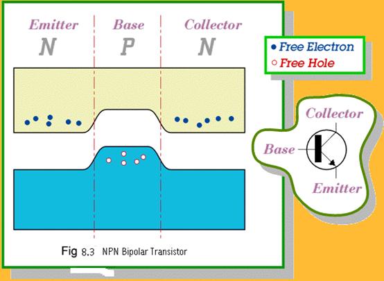
The diagram
above shows the energy levels in an NPN transistor when there are no externally applying any voltages. We can see
that the arrangement looks like a back-to-back pair of PN Diode junctions with
a thin P-type filling between two N-type slices of ‘bread’. In each of the
N-type layers conduction can take place by the free movement of electrons in
the conduction band. In the P-type (filling) layer conduction can take place by
the movement of the free holes in the valence band. However, in the absence of
any externally applied electric field, we find that depletion zones form
at both PN-Junctions, so no charge wants to move from one layer to another.
Figure 8.4 Biased Collector-Base junction
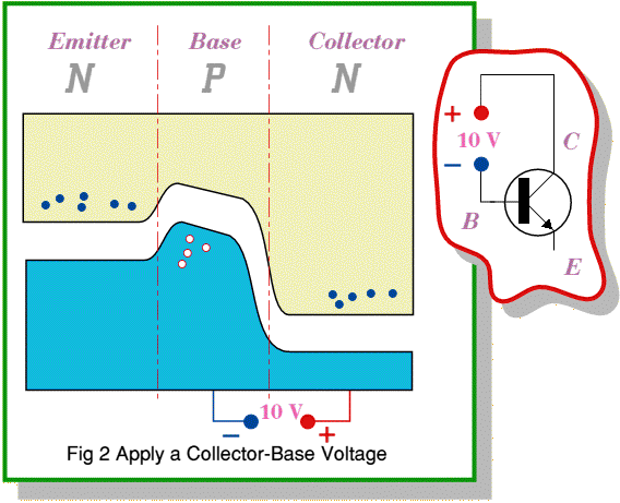
Looking at figure 8.4, we can see what happens when we
apply a moderate voltage between the Collector and Base parts of the
transistor. The polarity of the applied voltage is chosen to increase the force
pulling the N-type electrons and P-type holes apart. (i.e. we make the
Collector positive with respect to the Base.) This widens the depletion zone
between the Collector and base and so no current will flow. In effect we have
reverse-biased the Base-Collector diode junction. The precise value of the
Base-Collector voltage we choose doesn’t really matter to what happens provided
we don’t make it too big and blow up the transistor! So for the sake of example
we can imagine applying a 10 Volt Base-Collector voltage.
If we apply a tiny forward bias to the base emitter junction, big changes will happen.
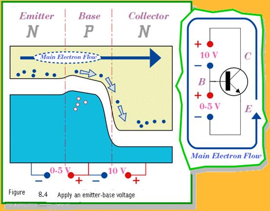
The relatively small Emitter-Base voltage, figure 8.4 ,
whose polarity is designed to forward-bias the Emitter-Base junction ‘pushes’
electrons from the Emitter into the Base region and sets up a current flow
across the Emitter-Base boundary. Once the electrons have managed to get into
the Base region they can respond to the attractive force from the
positively-biased Collector region. As a result the electrons which get into
the Base move swiftly towards the Collector and cross into the Collector
region. Hence we see a Emitter-Collector current whose magnitude is set by the
chosen Emitter-Base voltage we have applied. To maintain the flow through the
transistor we have to keep on putting ‘fresh’ electrons into the emitter and
removing the new arrivals from the Collector. Hence we see an external current
flowing in the circuit.
The precise value of the chosen Emitter-Base voltage isn’t too important to our
argument here, but it does determine the amount of current we’ll see.
For the sake of example we’ve chose half a volt although the generally accepted
figure for turn on voltage is 0.6-.7 volt.
Remember silicon diodes? Since
the Emitter-Base junction is a PN diode we can expect to see a current when we
apply forward voltages of this sort of size. In practice with a Bipolar
transistor made using Silicon we can expect to have to use an Emitter-Base
voltage in the range from around a half volt up to almost one volt. Higher
voltages tend to produce so much current that they can destroy the transistor!
It is worth noting that the magnitude of the current we see isn’t really affected
by the chosen Base-Collector voltage. This is because the current is mainly set
by how easy it is for electrons to get from the Emitter into the Base region.
Most (but not all!) the electrons that get into the Base move straight on into
the Collector provided the Collector voltage is positive enough to draw them
out of the Base region. That said, some of the electrons get ‘lost’ on the way
across the Base. This process is illustrated below:
Figure 8.5 Some electrons fall into hole
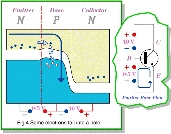
As we can see from figure 8.5, some of the free electrons crossing the Base
encounter a hole and ‘drop into it’. As a result, the Base region loses one of
its positive charges (holes) each time this happens. If we didn’t do anything
about this we’d find that the Base potential would become than
the Emitter Current more negative (i.e. ‘less positive’ because of the removal
of the holes) until it was negative enough to repel any more electrons from
crossing the Emitter-Base junction. The current flow would then stop.
To prevent this happening we use the applied Emitter-Base voltage to remove the
captured electrons from the Base and maintain the number of holes it contains.
This has the overall effect that we see some of the electrons which enter the
transistor via the Emitter emerging again from the Base rather than the
Collector. For most practical Bipolar Transistors we keep the base region part
of the sandwich really narrow and so only about 1% of the free electrons which
try to cross Base region get caught in this way. Hence we see a Base Current, IB,
which is typically around one hundred times smaller, IE.
Figure 8.6 Current gain (Beta) view of transistor
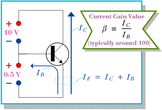
Viewed from the outside world we can describe the transistor’s behavior in
terms of a Current Gain, Beta. This is defined in terms of the ratio of
the number of electrons which manage to cross the transistor to those which get
caught. We can now treat the transistor as a Current Amplifier since
when we put ‘in’ (i.e. into the Base) a current, IB, we get ‘out’
(i.e. from the Emitter and Collector) a current, IC or IB,
which is much larger and whose value we can control by altering IB. We are now in the business of being able to
use the transistor as a switch or current amplifier.
Figure 8.7 Conventional view of transistor
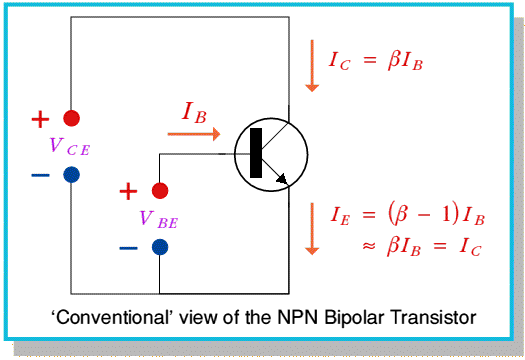
This leads us to the conventional view of Bipolar Transistors as they are
represented in most electronics text books. The diagram above shows two
changes: We now refer the Collector potential to the Emitter (VCE)
rather than to the Base, and we now represent the current in conventional terms
- passing from positive to negative. Since the precise Collector voltage doesn’t
have much effect on the currents, moving the place we reference it from isn’t
very important and this new view is more convenient in practice. Changing to
conventional (positive to negative) current flow allows us to fit in with the
normal view of electronics. Note also that, for simplicity, we can normally
assume that the values of the Collector and Emitter currents are essentially
identical since they only differ by a percent or so.
By remembering that the Base-Emitter is a forward biased diode junction and
taking the above description into account we can formulate two rough ‘rules of
thumb’ for the behavior of a Bipolar Transistor when using it as an amplifier,
etc. A more precise picture is got at by looking up the current gain HFE in a manufacturers’ catalogue.
These vary from about 20 -1000. They are generally lower for power transistors
and higher for small signal low current transistors.
· The Base-Emitter voltage, VBE will always be about half to 0.7 volt.
· The currents, IE = IC = 100×IB
·
More accurately IC
= HFE x IB
Types of transistor
|
|
|
|
Figure 8.8 Transistor
circuit symbols |
|
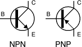
As we have seen there are two types of standard transistors, NPN and PNP, with different circuit symbols. The letters refer to the layers of semiconductor material used to make the transistor. Most transistors used today are NPN because this is the easiest type to make from silicon. This page is mostly about NPN transistors and if you are new to electronics it is best to start by learning how to use these first.
The leads are
labeled base (B), collector (C) and emitter (E). Below:
Figure 8.9
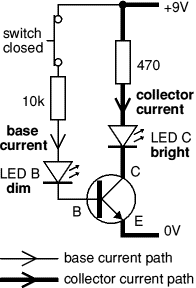 Practical
Transistor currents
Practical
Transistor currents
Figure 8.9 illustrates the fact that there is no
need to use two batteries as in our theoretical explanation. Properly chosen resistors do the trick. The diagram shows
the two current paths through a transistor. You can build this circuit with two
standard 5mm red LEDs and any general purpose low power NPN transistor (typical
manufactures’ codes being; BC108, BC182 or BC548 for example).
As we have seen from the theory, the small base current controls the larger collector current.
When the switch is closed, a small current will flow into the base (B) of the transistor. It is just enough to make LED B glow dimly. The transistor amplifies this small current to allow a larger current to flow through from its collector (C) to its emitter (E). This collector current is large enough to make LED C light brightly.
When the switch is open no base current flows, so the transistor switches off the collector current. Both LEDs are off.
·
This arrangement where the emitter
(E) is in the controlling circuit (base current) and in the controlled circuit
(collector current) is called common emitter mode. It is the most widely
used arrangement for transistors so it is the one to learn first.
Figure 8.10
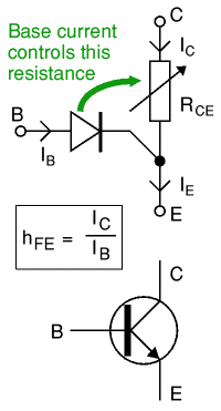
Functional model of an NPN transistor
You may have found the operation of a transistor difficult to understand in terms of its internal structure. If so, it may be more helpful to use the functional model figure 8.10:
· The base-emitter junction behaves like a diode.
· A base current IB flows only when the voltage VBE across the base-emitter junction is 0.7V or more.
· The small base current IB controls the large collector current Ic.
·
Ic = hFE × IB
(unless the transistor is full on and saturated)
hFE is the current gain (strictly the DC current gain), a typical
value for hFE is 100 (it has no units because it is a ratio)
· The collector-emitter resistance RCE is controlled by the base current IB:
- IB = 0 RCE = infinity transistor off
- IB small RCE reduced transistor partly on
- IB increased RCE = 0 transistor full on (‘saturated’)
Additional notes:
· A resistor is needed in series with the base connection to limit the base current IB and prevent the transistor being damaged.
· Transistors have a maximum collector current Ic rating.
· The current gain hFE can vary widely, even for transistors of the same type!
· A transistor that is full on (with RCE = 0) is said to be ‘saturated’.
· When a transistor is saturated the collector-emitter voltage VCE is reduced to almost 0V.
· When a transistor is saturated the collector current Ic is determined by the supply voltage and the external resistance in the collector circuit, not by the transistor’s current gain. As a result the ratio Ic/IB for a saturated transistor is less than the current gain hFE.
· The emitter current IE = Ic + IB, but Ic is much larger than IB, so roughly IE = Ic.
|
Figure
8.11 |
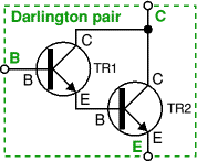
Darlington pair
This is two transistors connected together so that the current amplified by the first is amplified further by the second transistor. The overall current gain is equal to the two individual gains multiplied together:
(hFE1 and hFE2 are the gains of the individual
transistors)
This gives the
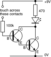
Figure 8.12 Darlington Pair as a touch switch
Using a transistor as a
switch to control large currents
When a transistor
is used as a switch it must be either OFF or fully ON. In the
fully ON state the voltage VCE across the transistor is almost zero
and the transistor is said to be saturated because it cannot pass any
more collector current Ic. The output 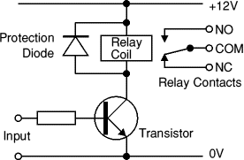 device switched by the transistor is usually called the ‘load’.
The power developed in a switching transistor is very small:
·
· Figure 8.12 Transistor relay driver with protection diode
· In the OFF state: power = Ic × VCE, but Ic = 0, so the power is zero.
· In the full ON state: power = Ic × VCE, but VCE = 0 (almost), so the power is very small.
This means that the transistor should not become hot in use and you do not need to consider its maximum power rating. The important ratings in switching circuits are the maximum collector current Ic(max) and the minimum current gain hFE(min). The transistor’s voltage ratings may be ignored unless you are using a supply voltage of more than about 15V. A much larger current can be controlled or switched by the relay contacts.
Protection diode
If the load is a
motor, relay or solenoid (or any other device with a coil)
a diode must be
connected across the load to protect the transistor (and chip) from damage when
the load is switched off. The diagram shows how this is connected ‘backwards’
so that it will normally NOT conduct. Conduction only occurs when the load is
switched off, at this moment current tries to continue flowing through the coil
and it is harmlessly diverted through the diode. Without the diode no current
could flow and the coil would produce a damaging high voltage ‘spike’ in its
attempt to keep the current flowing.
When to use a relay to drive an
output device
|
|
|
|
|
Figure 8.13 Relays
|


Transistors cannot switch AC or high
voltages (such as mains electricity) and they are not usually a good choice for
switching large currents (> 5A). In these cases a relay will be
needed, but note that a low power transistor may still be needed to switch the
current for the relay’s coil! Relays use an
electromagnetic coil to move the poles of a switch when powered. There are
three pairs of connections known as common, normally open and normally closed.
Advantages of relays:
· Relays can switch AC and DC, transistors can only switch DC.
· Relays can switch high voltages, transistors cannot.
· Relays are a better choice for switching large currents (> 5A).
· Relays can switch many contacts at once.
Disadvantages of relays:
· Relays are bulkier than transistors for switching small currents.
· Relays cannot switch rapidly; transistors can switch many times per second.
· Relays use more power due to the current flowing through their coil.
· Relays require more current than many chips can provide, so a low power transistor may be needed to switch the current for the relay’s coil.
Connecting a transistor to the output from a chip
Most chips cannot supply large output currents so it may be necessary to use a transistor to switch the larger current required for output devices such as lamps, motors and relays. The 555 timer chip which we shall meet soon is unusual because it can supply a relatively large current of up to 200mA which is sufficient for some output devices such as low current lamps, buzzers and many relay coils without needing to use a transistor.
A transistor can also be used to enable a chip connected to a low voltage supply (such as 5V) to switch the current for an output device with a separate higher voltage supply (such as 12V). The two power supplies must be linked, normally this is done by linking their 0V connections. In this case you should use an NPN transistor.
A resistor RB is required to limit the current flowing into the base of the transistor and prevent it being damaged. However, RB must be sufficiently low to ensure that the transistor is thoroughly saturated to prevent it overheating, this is particularly important if the transistor is switching a large current (> 100mA). A safe rule is to make the base current IB about five times larger than the value which should just saturate the transistor.
Choosing a suitable
NPN transistor
The circuit
diagram shows how to connect an NPN transistor; this will switch on the
load when the chip output is high. To get the opposite action, with the
load switched on when the chip output is low (0V) you can use a PNP transistor.
The procedure below explains how to choose a suitable
switching transistor.
|
|
|
Figure 8.14 NPN
transistor switch |
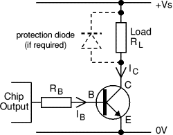
The transistor’s maximum collector current Ic(max) must be greater than the load current Ic.
|
load current Ic = |
supply voltage Vs |
|
load resistance RL |
The transistor’s minimum current gain hFE(min) must be at least five times the load current Ic divided by the maximum output current from the chip.
|
hFE(min) >
5 × |
load current Ic |
|
max. chip current |
Choose a transistor which meets these
requirements and make a note of its properties: Ic(max) and hFE(min).
Technical data for some popular transistors is available in manufacturers’
catalogues.
KEY POINTS
1.
Calculate an approximate value for the base resistor:
|
RB = |
Vc × hFE |
where Vc = chip supply voltage
|
|
5 × Ic |
2. For a simple circuit
where the chip and the load share the same power supply (Vc = Vs) you
may prefer to use: RB = 0.2 × RL × hFE
3. Then
choose the nearest standard value for the base resistor.
4. Finally, remember that if the load is a motor or relay coil a protection diode is required.
Worked Example
The output from a 4000 series CMOS chip is required to operate a relay with a
100![]() coil.
coil.
The supply voltage is 6V for both the chip and load. The chip can supply a
maximum current of 5mA.
1.
Load current = Vs/RL = 6/100 = 0.06A = 60mA,
so transistor must have Ic(max) > 60mA.
2.
The maximum current from the chip is 5mA, so transistor
must have hFE(min) > 60
(5 × 60mA/5mA).
3.
Choose general purpose low power transistor BC182 with Ic(max) = 100mA
and hFE(min) = 100.
4.
RB = 0.2 × RL × hFE = 0.2
× 100 × 100 = 2000![]() . so choose RB = 1k8 or 2k2.
. so choose RB = 1k8 or 2k2.
5.
The relay coil requires a protection
diode.
Transistor inverter
(NOT gate)
As we saw in Chapter 7, inverters (NOT gates) are available on logic chips but if you only require one inverter it is usually as easy to use the circuit given in figure 8.15. The output signal (voltage) is the inverse of the input signal:
- When the input is high (+Vs) the output is low (0V).
- When the input is low (0V) the output is high (+Vs).
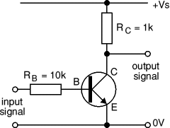
Figure 8.15 NPN Bipolar as a NOT GATE
Any general
purpose low power NPN transistor can be used. For general use RB = 10k![]() and RC = 1k
and RC = 1k![]() , then the inverter output can be
connected to a device with an input impedance (resistance) of at least 10k
, then the inverter output can be
connected to a device with an input impedance (resistance) of at least 10k![]() such as a logic chip or a 555 timer
(trigger and reset inputs).
such as a logic chip or a 555 timer
(trigger and reset inputs).
If you are connecting the inverter
to a CMOS logic chip input (very high impedance) you can increase RB
to 100k![]() and RC to 10k
and RC to 10k![]() , this will reduce the current used
by the inverter.
, this will reduce the current used
by the inverter.
The
NPN transistor as an audio amplifier
The arrangement shown in
figure 8.16 is often called the common emitter amplifier because the
input voltage to the transistor appears between the base & emitter, and the
output voltage appears between the collector & emitter — i.e. the emitter
terminal is shared by (or ‘common to’) the input and output.
Note. ![]() ,
, ![]() , and
, and ![]() are the voltages between each of the
transistor base, collector, and emitter terminals and the ‘ground’ (zero
volts). They aren't the same thing as
are the voltages between each of the
transistor base, collector, and emitter terminals and the ‘ground’ (zero
volts). They aren't the same thing as ![]() or
or ![]() which are the voltages from base-to-emitter
and collector-to-emitter more usually associated with manufactures’
specifications. The diagram also shows
the input and output signal AC voltages,
which are the voltages from base-to-emitter
and collector-to-emitter more usually associated with manufactures’
specifications. The diagram also shows
the input and output signal AC voltages, ![]() and
and ![]() . These aren't equal to
. These aren't equal to ![]() and
and ![]() because the 0·1
because the 0·1![]() F capacitors block any d.c. connection
between these potentials.) If puzzled see section of this book on Capacitors.
F capacitors block any d.c. connection
between these potentials.) If puzzled see section of this book on Capacitors.
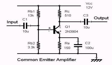
Figure 8.16 Class A Common Emitter Amplifier
It could actually be VERY complicated to work out all the resistor values if we followed the rigorous mathematical route to deal with both the D.C. and A.C. conditions in the circuit. However the same old rule of thumb conditions apply to the transistor which we have met previously. The base bias resistors shown in figure 8.16 must be chosen to satisfy point (1) below. That is the transistor must be slightly turned on that is conducting some D.C current all the time. This is known a class A.
- The base-emitter voltage will always be about 0·6 Volts (or 0·6
for a PNP transistor).
- The current gain (the
 value) will be a few hundred.
 - The large value means that
 , so we can assume that
 Figure
8.17
Figure
8.17
In figure 8.17 only a skeleton cirucit is
shown. We can see how the output
waveform is a perfectly ampliifed replica of the input. In a Class A circuit, the transistor is biased such that the device is always
conducting to some extent, and is operated over the most linear portion of its
characteristic curve (known as its transfer
characteristic or transconductance
curve). Because the device is always conducting, even if there is no input at
all, power is wasted. This is the reason for its efficiency is quite low. The input A.C. signal merely adds to and
subtracts from the base bias. The output
signal V out merely adds to
and sutracts from Vc. In the
simplest case Re is used to limit the
current through the transistor to stop it getting thremal runaway.
MOSFETS.
If output
currents larger than 1A are needed and high speed switching is desired which draws virtually no current from the
logic gate’s output, then a high power
transducer driver can be built using a MOSFET (metal oxide field effect
transistor).
Like
bipolar transistors FET's have three legs but they are called the gate, source
and drain. Unlike bipolar transistors
however MOSFET's have very high input impedance and require only a very small
gate current to operate. In the true sense of the word they a voltage operated
rather the current operated devices.
depletion mode. IGFET is a related, more general term meaning insulated-gate
field-effect transistor, and is almost synonymous with "MOSFET",
though it can refer to FETs with a gate insulator that is not oxide. Some
prefer to use "IGFET" when referring to devices with polysilicon
gates, but most still call them MOSFETs.
Usually the semiconductor of choice is silicon, but some
chip manufacturers, most notably IBM, have begun to use a mixture of silicon and germanium (SiGe) in MOSFET
channels. Unfortunately, many semiconductors with better electrical properties
than silicon, such as gallium arsenide, do not form good gate oxides and
thus are not suitable for MOSFETs.
The gate terminal is a layer of polysilicon
(polycrystalline silicon; why polysilicon is used will be explained below)
placed over the channel, but separated from the channel by a thin insulating
layer of what was traditionally silicon dioxide, but more advanced technologies
used silicon oxynitride. When a voltage is applied between the gate and source
terminals, the electric field generated penetrates through the oxide and
creates a so-called "inversion channel" in the channel underneath.
The inversion channel is of the same type — P-type or N-type — as the source
and drain, so it provides a conduit through which current can pass. Varying the
voltage between the gate and body modulates the conductivity of this layer and makes it
possible to control the current flow between drain and source. Devices
where a gate voltage enhances the channel are called Enhancement mode and
devices where the gate voltage pinches off the channel and stops current flow
are called Depletion Mode
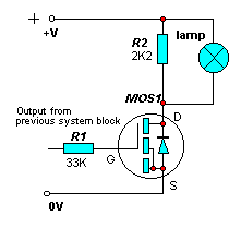 Figure 8.18 Mosfet as a transducer driver
Inductive Switching Issues
The switching of inductive loads can be very hazardous for the health of the switching device. While mechanical switches can cope with the arcing between the contacts at the expense of operating life, a semiconductor device will almost certainly be killed by the large voltage transient at turn off. The simplest method to solve this problem is to use a commutating, clamp diode or protection diode across the inductive component. The diagram below shows the layout of a diode clamped coil with MOSFET switch.
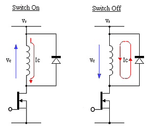
Figure 8.19
When the switch is conducting, the diode is reverse bias and therefore no current exists in the diode branch. If the MOSFET is turned off quickly, the collapsing magnetic flux of the coil induces a voltage in the coil which tries to maintain the current. The faster the current is switched off, the larger is the induced voltage. Without a commutating or protection diode the induced voltage could reach several hundreds or even thousands of volts, certain death for the MOSFET, if the pulse exceeds the rated avalanche energy. Basically the commutating diode provides a low resistance path for the induced voltage to drive the current. The voltage only has to rise to a level which is enough to reach the conducting voltage of the diode, usually around 1V. This keeps the MOSFET happy and ready for its next switching action. While this is certainly an effective means of limiting the turn off transient voltage, it isn't necessarily the best in terms of turn off speed. Ideally we want the current in the coil to turn off as quickly as possible. The simple commutating diode is sufficient for an A-level understanding but in reality is some distance from the ideal goal. If we want the current to decay faster we need to let the induced voltage reach a higher value. The absolute maximum we can allow it to rise depends on the voltage rating of the device. Suppose we are using a 60V MOSFET and a 40V supply, the largest induced voltage allowable is then 20V. One possibility is to connect a resistor in series with the diode. The specific value would need to be determining according to the coil current at turn off, the supply voltage, and the maximum device voltage. Another would be to use a zener voltage clamp across the MOSFET.
CHAPTER
NINE: SIMPLE OUTPUT DEVICES
In reality output devices are simply chosen for
the job in hand.
With an alarm
system you may want a visible warning for the deaf, i.e. a bright strobing lamp of some sort and you may
want a loud audible siren, bell or
buzzer.
To create movement
as say in robot or model aircraft the output device will be called an actuator
and may be motor. Motors come in various types which will be discussed later
in this book. For more powerful
movement hydraulic actuators may be
needed.
With an amplifier
you may want headphones or a loudspeaker
as an output device.
With an on –off warning light for a piece of
equipment or a low battery voltage indicator a
single LED (Light Emitting diode) will suffice .
With a clock
or timer or counter you may want a seven
segment LED display or an LCD display.
With a more sophisticated information system
such as a motorway warning gantry
you may want a dot matrix display.
The purpose of this Chapter then is to look at
the construction and operation of output devices which in turn relates to how they
must be interfaced, that is connected to the previous stage, and driven.
Filament
bulbs
Connecting filament bulbs or lamps is easy,
they simply act as resistive loads and the maximum current they consume is
worked out by considering their resistance when cold. So provided the output driver device or
sub-system you employ can deliver this current there is no problem in
interfacing the device.
|
|
|
|
Bulbs are relatively
easy to use. A bulb will be rated according to the maximum safe voltage and
the current that will flow at this voltage. A bulb rated at 6 V, 0.06A
will have a resistance of 100 ohms when it is working at normal brightness. |
|
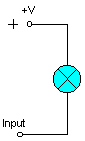
The input terminal would connect to
the collector of a NPN or Drain of a MOSFET driver.
Electric Bells.
When the switch is pushed closed the
circuit is completed and current flows through the coil. The iron striker is attracted
to the electromagnet and strikes the bell.As the striker moves towards the bell, the contact is broken. Current stops
flowing through the coil which loses its magnetism. The spring returns the striker
to its original position which makes a new contact and so electricity flows
again. Back to the start and the cycle repeats itself. The bell will continue to ring as long as
the switch held closed. The bell is an
inductive load and must be interfaced according to the 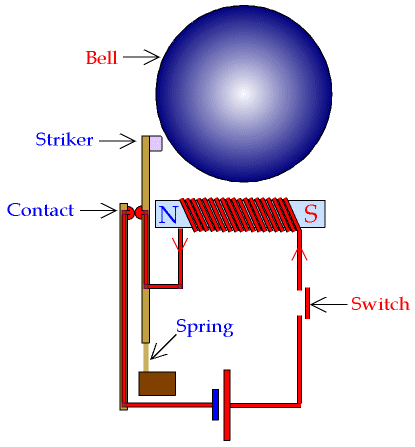
Figure 9.2 Electric
methods described in
Chapter 8 for such loads.
Buzzers
Buzzers come in
several different types. Depending on the type will depend on the
interfacing. Figure 9.3 shows an ageing
D.C buzzer, alongside its modern counterpart, both of which operate on a
similar principle to the electric bell. A.C. buzzers are also possible. D.C. Buzzers must be treated as inductive
loads. A.C. Buzzers must be powered
through a relay.

Figure
9.3 Buzzers ancient and modern
Buzzers based on vibrating piezoelectric elements are also possible, see figure 9.3.
A transistor circuit to drive such a buzzer is shown in figure 9.4.
Piezo transducer
|
Figure
9.4 |
|
Piezo
transducer |
|
|
|
circuit symbol |

Piezo transducers are output transducers which convert an electrical signal to sound. They require a driver circuit (such as a 555 astable) to provide a signal and if this is near their natural (resonant) frequency of about 3kHz they will produce a particularly loud sound.
Piezo transducers require a small current, usually less than 10mA, so they can be connected directly to the outputs of most ICs. They are ideal for buzzes and beeps, but are not suitable for speech or music because they distort the sound. They are sometimes supplied with red and black leads, but they may be connected either way round. PCB-mounting versions are also available. Piezo transducers can also be used as input transducers for detecting sudden loud noises or impacts, effectively behaving as a crude microphone
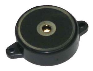 Fig 9.5
A Piezo-buzzer
Fig 9.5
A Piezo-buzzer
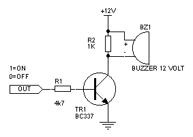
Figure
9.6 Circuit to drive piezo-buzzer from Logic source.
Integrated
or Complete Audible Warning Devices (CAWD)
Besides bells and buzzers, these days a large range of audio warning devices is available which have their own integral circuitry capable of producing a large variety of high level sounds up to in some cases > 120 decibels, in other words almost ear splitting sound! You should always refer to the manufacturers’ data sheet for connection of such devices which are often polarity and voltage conscious.
The circuits in these devices often use a combination of logic gates and mosfets to produces very high voltage 200-300 volt short duration pulses which are sent to specially reinforced piezo-electric sounder elements. Conventional loudspeakers cannot stand such high voltages.
Dynamic Loudspeaker Principle
A
current-carrying wire in a magnetic field experiences a magnetic
force perpendicular to the wire. In practice the wire is wrapped into a
coil attached to a stiffened paper cone which then vibrates back and forth in
sympathy with the induced movement. See figure 9.7
|
. |
|
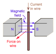
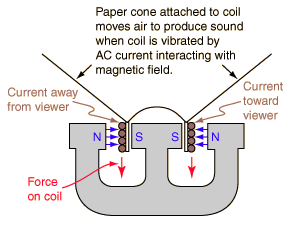
Figure 9.7 Loudspeaker Construction and principle
Figure 9.8 Actual loudspeaker 
Loudspeakers, figure 9.8, are output
transducers which convert an electrical signal to sound. Usually they are
called 'speakers'. They require a driver circuit, such as a 555 astable or an
audio amplifier, to provide a signal. There is a wide range available, but for
many electronics projects a 300mW miniature loudspeaker is ideal. This type is
about 70mm diameter and it is usually available with resistances of 8![]() and 64
and 64![]() . If a project specifies a 64
. If a project specifies a 64![]() speaker you must use this higher
resistance to prevent damage to the driving circuit.
speaker you must use this higher
resistance to prevent damage to the driving circuit.
Most circuits used to drive loudspeakers produce an audio (AC) signal since sounds, voices and music are essentially time varying fluctutations it is necessary as we have seen for amplifiers to separate out these currents and voltages present. Alternating components from any quiescent or standing D.C. which is combined with a constant DC signal. The DC will make a large current flow through the speaker due to its low resistance, possibly damaging both the speaker and the driving circuit. To prevent this happening a large value electrolytic capacitor is connected in series with the speaker, this blocks DC but passes audio (AC) signals. See capacitors
Loudspeakers may be connected either way round except in stereo circuits when the + and - markings on their terminals must be observed to ensure the two speakers are in phase.
Correct polarity must always be observed for large speakers in cabinets because the cabinet may contain a small circuit (a 'crossover network') which diverts the high frequency signals to a small speaker (a 'tweeter') because the large main speaker is poor at reproducing them.
Miniature loudspeakers can also be
used as a microphone and they work surprisingly well, certainly well enough for
speech in an intercom system for example.
 Figure 9.9 speaker circuit symbol
A simple
amplifier to boost the audio line out from a computer is shown in figure 9.10 ,
note how the loudpseaker is A.C. coupled to the circuit through a 470
micro-farad capacitor.
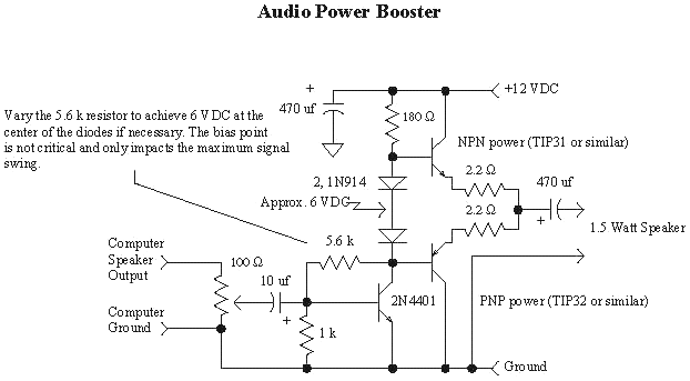
Figure 9.10 Computer audio amplifier
We will revist audio amplifiers in a later section
of this book, see filters and push-pull output stages.
LEDS (Light Emitting
Diodes)
Light
emitting diodes or LEDs are polarized devices and must be connected the right
way round in a circuit. Since the maximum voltage to be applied across an LED
is about 2V they almost always have a resistor connected in series. The value of
the resistor is calculated from the voltage of the power supply and the current
required by the LED.
LEDs come in three main colours: red, yellow and
green. Blue LED's are available but are very expensive. There can be bought in
a wide range of sizes and shapes - look at suppliers’ catalogues for more
details
|
|
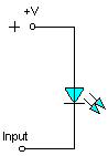
Figure 9.11 LED symbol.
Example:
![]() Circuit symbol:
Circuit symbol:
![]()
Function
LEDs emit light when an electric current passes through them. They are much more efficient than filament bulbs and require less current generally about 10-20 mA.
Connecting and
soldering
LEDs must be connected the correct way round, the diagram is labeled a or + for anode and k or - for cathode (yes, it really is k, not c, for cathode!). The cathode is the short lead and there may be a slight flat on the body of round LEDs. If you can see inside the LED the cathode is the larger electrode (but this is not an official identification method).
LEDs can be damaged by heat when
soldering, but the risk is small unless you are very slow. No special
precautions are needed for soldering most LEDs.
Testing an LED
Never connect an LED directly to a
battery or power supply!
It will be destroyed almost instantly because too much current will pass
through and burn it out.
Figure 9. 12 Coloured LEDS
For quick testing purposes a 1k![]() resistor is suitable as a current
limiter for most LEDs if your supply voltage is 12V or less. Remember to
connect the LED the correct way round! The flat on its body is the negative or
cathode connection.
resistor is suitable as a current
limiter for most LEDs if your supply voltage is 12V or less. Remember to
connect the LED the correct way round! The flat on its body is the negative or
cathode connection.
Colours
of LEDs
LEDs are available in red, orange, amber, yellow, green, and blue and white. Blue and white LEDs are much more expensive than the other colours.
The colour of an LED is determined
by the semiconductor material, not by the colouring of the 'package' (the
plastic body). LEDs of all colours are available in uncoloured packages which
may be diffused (milky) or clear (often described as 'water clear'). The
coloured packages are also available as diffused (the standard type) or
transparent.
Tri-colour LEDs
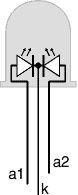
Figure 9.13
Tricolour LED
The most popular type of tri-colour LED has a red and a green LED combined in one package with three leads. They are called tri-colour because mixed red and green light appears to be yellow and this is produced when both the red and green LEDs are on.
The diagram shows the construction
of a tri-colour LED. Note the different lengths of the three leads. The centre
lead (k) is the common cathode for both LEDs, the outer leads (a1 and a2) are
the anodes to the LEDs allowing each one to be lit separately, or both together
to give the third colour.
Bi-colour LEDs
A bi-colour LED has two LEDs wired in 'inverse parallel' (one forwards, one backwards) combined in one package with two leads. Only one of the LEDs can be lit at one time and they are less useful than the tri-colour LEDs described above.
Sizes,
Shapes and Viewing angles of LEDs
LEDs are available in a wide variety of sizes and shapes. The 'standard' LED has a round cross-section of 5mm diameter and this is probably the best type for general use, but 3mm round LEDs are also popular.
Round cross-section LEDs are frequently used and they are very easy to install on boxes by drilling a hole of the LED diameter, adding a spot of glue will help to hold the LED if necessary. LED clips are also available to secure LEDs in holes. Other cross-section shapes include square, rectangular and triangular.
As well as a variety of colours, sizes and shapes, LEDs also vary in their viewing angle. This tells you how much the beam of light spreads out. Standard LEDs have a viewing angle of 60° but others have a narrow beam of 30° or less.
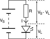
Figure 9.14 Calculating
an LED resistor value
Exam Topic
An LED must have a resistor connected in series to limit the current through the LED, otherwise it will burn out almost instantly.
The resistor value, R is given by:
|
R = (VS - VL)
/ I |
VS = supply voltage
VL = LED voltage (usually 2V, but 4V for blue and white LEDs)
I = LED current (e.g. 20mA), this must be less than the maximum permitted
If the calculated value is not available choose the nearest standard resistor value which is greater, so that the current will be a little less than you chose. In fact you may wish to choose a greater resistor value to reduce the current (to increase battery life for example) but this will make the LED less bright.
For example
If the supply
voltage VS = 9V, and you have a red LED (VL = 2V),
requiring a current I = 20mA = 0.020A,
R = (9V - 2V) / 0.02A = 350![]() , so choose 390
, so choose 390![]() (the nearest standard value which is
greater).
(the nearest standard value which is
greater).
Working out the LED resistor formula using Ohm's law
Ohm's law says
that the resistance of the resistor, R = V/I, where:
V = voltage across the resistor (= VS - VL
in this case)
I = the current through the resistor
So R = (VS - VL) / I
In practice LEDS will often be driven
direct by small transistors, logic or timer I.C.S.
|
|
|
Figure
9.15 |
|
Driving
a LED |
7 Segment Displays
LED displays are packages of many LEDs arranged in a pattern, the most familiar pattern being the 7-segment displays for showing numbers (digits 0-9). The pictures below illustrate some of the popular designs:
|
|
|
|
|
|
Bargraph |
7-segment |
Starburst |
Dot matrix |
|
Figure
9.16 Various LED Displays |
|||

Pin connections of LED displays
|
|
|
Figure 9.17 Pin
connections diagram |
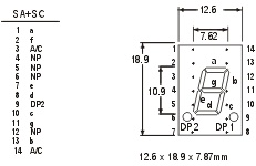
There are many types of LED display and a supplier's catalogue
should be consulted for the pin connections. The diagram on the right shows an
example from a manufactures’ catalogue; like many 7-segment displays, this
example is available in two versions: Common Anode (SA) with all the LED anodes
connected together and Common Cathode (SC) with all the cathodes connected
together. Letters a-g refers to the 7 segments, A/C is the common anode or
cathode as appropriate (on 2 pins). Note that some pins are not present (NP)
but their position is still numbered.
Exercise
Try to work out for yourselves which segments need
to be illuminated to make numbers 0-9. Assume the device has a common cathode. Which
boxes need a logic1 in the grid?
|
|
1 |
2 |
3 |
4 |
5 |
6 |
7 |
8 |
9 |
0 |
|
a |
|
|
|
|
|
|
|
|
|
|
|
b |
|
|
|
|
|
|
|
|
|
|
|
c |
|
|
|
|
|
|
|
|
|
|
|
d |
|
|
|
|
|
|
|
|
|
|
|
e |
|
|
|
|
|
|
|
|
|
|
|
f |
|
|
|
|
|
|
|
|
|
|
|
g |
|
|
|
|
|
|
|
|
|
|
Figure 9.18 7 Segment Exercise
Solenoid
A solenoid consists of a coil of wire around a
ferrous core. Solenoids are
similar to relays but instead of bringing about electrical switching they can
bring about linear mechanical movement which may or may not be of the latching
kind depending on the precise mechanical arrangement. This is because it converts the electrical signal into linear
kinetic energy.
Because the solenoid is an inductive component it
needs a protection diode in the same manner as the other inductive devices
discussed.
Motors
A
Some
The commutator is made up of a series of
separate sectors with insulation between them and, as the brushes pass from one
sector to another, there is a switching of current.
This rapid switching causes voltage spikes to appear on the power lines and this can disturb the working of the rest of the circuit. If electronic methods of suppression (usually a resistor in series with the motor and a capacitor across the terminals of the motor) are not successful, it may be necessary to use a separate power supply for the motor and switch it on through a relay.
CHAPTER 10: CAPACITORS
AND TIMING SUB-SYSTEMS
Imagine we build a burglar alarm. We might want the alarm siren to sound a series of beeps or whistles or warbles that stop after a given period. How would we do it?
We can use a special subsystem known as a 555 Timer IC which can be configured as either a pulse generator (Astable) or Timer (Monostable).
In order to understand how these sub-systems work one must first understand something about an electronic component known as a capacitor.
|
unpolarised
capacitor symbol |
|
|
|
polarised
capacitor symbol |
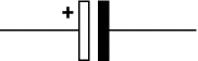
Capacitance
Capacitance (symbol C) is a measure of a capacitor's ability to store charge. A large capacitance means that more charge can be stored. Capacitance is measured in farads, symbol F. However 1F is very large for practical purposes, so prefixes as in figure 2.1 (multipliers) are used to show the smaller values,
- µ (micro) means 10-6 (millionth), so 1000000µF = 1F
- n (nano) means 10-9 (thousand-millionth), so 1000nF = 1µF Figure 10.1
- p (pico) means 10-12 (million-millionth), so 1000pF
= 1nF Capacitor
symbols
Charge
and Energy Stored
The amount of charge (symbol Q) stored by a capacitor is given by:
|
Charge, Q = C × V |
where: |
Q = charge in coulombs (C) |
When they store charge, capacitors are also storing energy:
|
Energy, E = ½QV = ½CV² where E = energy in joules (J). |
Note that capacitors return their
stored energy to the circuit. They do not 'use up' electrical energy by
converting it to heat as a resistor does. The energy stored by a capacitor is
much smaller than the energy stored by a battery so they cannot be used as a practical source of energy for most purposes,
although very large banks of high voltage capacitors can be
charged for use in heart defibrillators, for example.
Capacitive
Reactance Xc
Capacitors oppose A.C. current flow a little bit like resistors
oppose D.C. flow. Capacitive reactance (symbol Xc) is a measure of a
capacitor's opposition to AC (alternating current). Like resistance it is
measured in ohms,![]() , but reactance is more complex than
resistance because its value depends on the frequency (f) of the electrical
signal passing through the capacitor as well as on the capacitance, C. Also
reactance can’t be measured on a simple D.C. ohmmeter.
, but reactance is more complex than
resistance because its value depends on the frequency (f) of the electrical
signal passing through the capacitor as well as on the capacitance, C. Also
reactance can’t be measured on a simple D.C. ohmmeter.
|
Capacitive reactance, Xc
= |
1 |
where: |
Xc = reactance in ohms ( |
|
|
|||
|
2 |
The reactance Xc is large at low frequencies and small at high frequencies. For steady DC which is zero frequency, Xc is infinite (total opposition), hence the rule that capacitors appear to pass AC but block DC.
For example a 1µF capacitor has a
reactance of 3.2k![]() for a 50Hz signal, but when the
frequency is higher at 10kHz its reactance is only 16
for a 50Hz signal, but when the
frequency is higher at 10kHz its reactance is only 16![]() . We will meet these ideas again when we
consider audio filters.
. We will meet these ideas again when we
consider audio filters.
.
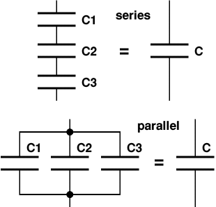 Capacitors
in Series and Parallel
Capacitors
in Series and Parallel
|
Combined capacitance (C) of |
1 |
= |
1 |
+ |
1 |
+ |
1 |
+ ... |
|
|
|
|
|
|||||
|
C |
C1 |
C2 |
C3 |
|
Combined capacitance (C) of |
C = C1 + C2 + C3 + ... |
Figure 10.2 Capacitors in series and parallel
The above formulae are often found in exam data sheets. If you are good at fractions you will see that a short cut if you have just two capacitors in series is called the product over sum rule
C= C1XC2/ (C1+C2)
Two or more capacitors are rarely deliberately connected in series in real circuits, but it can be useful to connect capacitors in parallel to obtain a very large capacitance, for example to smooth a power supply.
KEY POINT Note that these equations are the opposite way round for resistors
in series and parallel.
Charging
a capacitor
When a capacitor is connected straight to a battery or power supply it charges
instantaneously but the charging can be slowed down by resistor.
The capacitor (C) in the circuit diagram is being charged from a
supply voltage (Vs) with the current passing through a resistor (R). The
voltage across the capacitor (Vc) is initially zero but it increases as the
capacitor charges. The capacitor is fully charged when Vc = Vs. The
charging current (I) is determined by the voltage 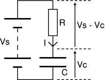 across the resistor (Vs - Vc):
Charging current, I = (Vs - Vc) / R (note that Vc is increasing) The capacitor (C) in the circuit diagram is being charged from a supply voltage (Vs) with the current passing through a resistor (R).
At first Vc = 0V so the initial current, Io = Vs / R
Figure
10.3 Capacitor charging circuit
Vc increases as soon as charge (Q)
starts to build up (Vc = Q/C), this reduces the voltage across the
resistor and therefore reduces the
charging current. This means that the rate of charging becomes progressively
slower.
|
time constant = R × C |
where: |
time constant is in seconds
(s) |
Example Calculations:
If R = 47k![]() and C = 22µF, then the time
constant, RC = 47k
and C = 22µF, then the time
constant, RC = 47k![]() × 22µF = 1.0s.
× 22µF = 1.0s.
If R = 33k![]() and C = 1µF, then the time constant,
RC = 33k
and C = 1µF, then the time constant,
RC = 33k![]() × 1µF = 33ms.
× 1µF = 33ms.
A large time constant means the
capacitor charges slowly. Note that the time constant is a property of
the circuit containing the
capacitance and resistance; it is not a property of a capacitor alone.
|
Graphs showing the current and |
|
|
|
Figure 10.4 Current in a charging capacitor |
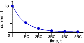
The time constant is the time
taken for the charging (or discharging) current (I) to fall to 1/e
of its initial value (Io). 'e' is the base of natural logarithms, an important
number in mathematics (like ![]() ). e = 2.71828 (to 6
significant figures) so we can roughly say that the time constant is the time
taken for the current to fall to 1/3 of its initial
value.
). e = 2.71828 (to 6
significant figures) so we can roughly say that the time constant is the time
taken for the current to fall to 1/3 of its initial
value.
After each time constant the current falls by 1/e (about 1/3). After 5 time constants (5RC) the current has fallen to less than 1% of its initial value and we can reasonably say that the capacitor is fully charged, but in fact the capacitor takes for ever to charge fully!
|
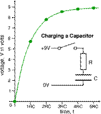 7V
7VThe bottom graph shows how the voltage (V) increases as the capacitor charges. At first the voltage changes rapidly because the current is large; but as the current decreases, the charge builds up more slowly and the voltage increases more slowly.
Because of the mathematics involved it is easier to remember just key points on the charging curve most examinations only call for these, which have been highlighted in yellow. For instance after 0.69 Time constants or 0.69 RC 50 % of total charge is reached or the
Figure 10.5 Voltage in a charging capacitor
capacitor has charged to exactly half the supply voltage. After one time constant (RC), the capacitor has charged to 63% of total charge or supply voltage.
After 5 time constants (5RC) the capacitor is almost fully charged with its voltage almost equal to the supply voltage. We can reasonably say that the capacitor is fully charged after 5RC, so this figure of 5RC is needed for exam recall, although really charging continues for ever (or until the circuit is changed).
Discharging
a capacitor
|
Graphs showing the current and |
|
|
|
|
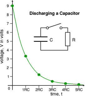
The top graph shows how the current (I) decreases as the capacitor discharges. The initial current (Io) is determined by the initial voltage across the capacitor (Vo) and resistance (R):
Initial current, Io = Vo / R.
Note that the current graphs are
the same shape for both charging and discharging a capacitor. This type of
graph is an example of exponential decay.
Key points discharge curve.
· To ½ charge or ½ terminal voltage in 0.69RC seconds
· To 37% (100-63) of charge or terminal voltage in RC seconds
· To zero in 5RC second
Figure 10.6 Discharging a capacitor
Where we might use a capacitor.
- For ‘AC Coupling’ between stages of an audio system and to connect a loudspeaker.
- Filtering - for example in the tone control of an audio system, see later
- Tuning - for example in a radio system, see later
- Storing energy - for example in a camera flash circuit.
Practical Capacitors
As we have seen capacitors store electric charge. They are used with resistors in timing circuits because it takes time for a capacitor to fill with charge. They are used to smooth varying DC supplies by acting as a reservoir of charge. They are also used in filter circuits because capacitors easily pass AC (changing) signals but they block DC (constant) signals.
Three prefixes (multipliers) are used, µ (micro), n (nano) and p (pico):
- µ means 10-6 (millionth), so 1000000µF = 1F
- n means 10-9 (thousand-millionth), so 1000nF = 1µF
- p means 10-12 (million-millionth), so 1000pF = 1nF
Values of capacitors are often harder to find because there are many types of capacitor with different labeling systems compared with simple resistor codes! In a good electronics lab a capacitance meter is thus a useful tool.
Capacitors split into two groups, polarised and unpolarised. Each group has its own circuit symbol.
Polarised
capacitors (large values, 1µF +)
Examples: 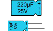
Figure 10.7 Polarised or electrolytic capacitors
Electrolytic Capacitors
Electrolytic capacitors are polarised and they must be connected the correct way round, at least one of their leads will be marked + or -. They are not damaged by heat when soldering.
There are two designs of electrolytic capacitors; axial where the leads are attached to each end (220µF in picture) and radial where both leads are at the same end (10µF in picture). Radial capacitors tend to be a little smaller and they stand upright on the circuit board.
It is easy to find the value of electrolytic capacitors because they are clearly printed with their capacitance and voltage rating. The voltage rating can be quite low (6V for example) and it should always be checked when selecting an electrolytic capacitor. If the project parts list does not specify a voltage; choose a capacitor with a rating which is greater than the project's power supply voltage. 25V is a sensible minimum for most battery circuits.
Tantalum Bead Capacitors
Tantalum bead capacitors are also polarised and have low voltage ratings like electrolytic capacitors. They are expensive but very small, so they are used where a large capacitance is needed in a small size.
Modern tantalum bead capacitors are printed with their capacitance and voltage in full. However older ones use a colour-code system which has two stripes (for the two digits) and a spot of colour for the number of zeros to give the value in µF. The
standard colour code is used, but for the spot, grey is used to mean × 0.01 and white means × 0.1 so that values of less than 10µF can be shown. A third colour stripe near the leads shows the voltage (yellow 6.3V, black 10V, green 16V, blue 20V, grey 25V, white 30V, pink 35V).
For example: blue, grey,
black spot means 68µF
For example: blue, grey, white spot means 6.8µF
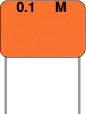 For example: blue, grey, grey spot means 0.68µF
 Unpolarised capacitors (small values, up
to 1µF)
Unpolarised capacitors (small values, up
to 1µF)
Examples:
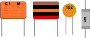
Circuit
symbol: 
Figure 10.8 Non-polarised capacitors.
Small value capacitors are unpolarised and may be connected either way round. They are not damaged by heat when soldering, except for one unusual type (polystyrene). They have high voltage ratings of at least 50V, usually 250V or so. Many small value capacitors have their value printed but without a multiplier, so you need to use experience to work out what the multiplier should be!
For example 0.1 means 0.1µF = 100nF.
Sometimes the multiplier is used
in place of the decimal point:
For example: 4n7 means 4.7nF.
Capacitor Number Code
A number code is often used on small capacitors where printing is difficult:
- the 1st number is the 1st digit,
- the 2nd number is the 2nd digit,
- the 3rd number is the number of zeros to give the capacitance in pF.
- Ignore any letters - they just indicate tolerance and voltage rating.
For example: 102 means 1000pF = 1nF (not 102pF!)
For example: 472J means 4700pF = 4.7nF (J means 5% tolerance).
|
Colour Code |
|
|
Colour |
Number |
|
Black |
0 |
|
Brown |
1 |
|
Red |
2 |
|
|
3 |
|
Yellow |
4 |
|
Green |
5 |
|
Blue |
6 |
|
Violet |
7 |
|
Grey |
8 |
|
White |
9 |
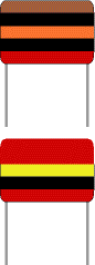 Capacitor Colour Code
A colour code was used on polyester capacitors for many years. It is now obsolete, but of course there are many still around. The colours should be read like the resistor code, the top three colour bands giving the value in pF. Ignore the 4th band (tolerance) and 5th band (voltage rating).
For example:
brown, black, orange means 10000pF = 10nF = 0.01µF.
Note that there are no gaps between the colour bands, so 2 identical bands actually appear as a wide band.
![]()
Figure 10.9 Capacitor color code
For example:
wide
red, yellow means 220nF = 0.22µF.
Polystyrene Capacitors
This type is rarely used now. Their value (in pF) is normally printed without units. Polystyrene capacitors can be damaged by heat when soldering (it melts the polystyrene!) so you should use a heat sink (such as a crocodile clip). Clip the heat sink to the lead between the capacitor and the joint.
Real
capacitor values (the E3 and E6 series)
You may have noticed that capacitors are not available with every possible value, for example 22µF and 47µF are readily available, but 25µF and 50µF are not!
Why is this? Imagine that you decided to make capacitors every 10µF giving 10, 20, 30, 40, 50 and so on. That seems fine, but what happens when you reach 1000? It would be pointless to make 1000, 1010, 1020, 1030 and so on because for these values 10 is a very small difference, too small to be noticeable in most circuits and capacitors cannot be made with that accuracy.
To produce a sensible range of capacitor values you need to increase the size of the 'step' as the value increases. The standard capacitor values are based on this idea and they form a series which follows the same pattern for every multiple of ten.
The E3 series (3 values for each
multiple of ten)
10, 22, 47, then it continues 100, 220, 470, 1000, 2200, 4700, 10000
etc.
Notice how the step size increases as the value increases (values roughly
double each time).
The E6 series (6 values for each
multiple of ten)
10, 15, 22, 33, 47, 68, then it continues 100, 150, 220, 330, 470, 680,
1000 etc.
Notice how this is the E3 series with an extra value in the gaps.
The E3 series is the one most frequently used for capacitors because many types cannot be made with very accurate values.
Silvered Mica Capacitors
For real precision work usually in the pico-farad ranges of capacitance, silvered mica capacitors are employed. The dielectric or insulating material in these capacitors is the naturally occurring mineral material mica. The electrodes are silver plated or sputtered directly onto the mica.
Variable
capacitors
|
|
|
Variable Capacitor Symbol |
|
|
|
Figure
10.10 Variable Capacitor |
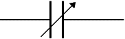
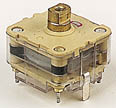
Variable capacitors are mostly used in radio tuning circuits and they are sometimes called 'tuning capacitors'. They have very small capacitance values, typically between 100pF and 500pF (100pF = 0.0001µF). The type illustrated usually has trimmers built in (for making small adjustments - see below) as well as the main variable capacitor.
Many variable capacitors have very short spindles which are not suitable for the standard knobs used for variable resistors and rotary switches. It would be wise to check that a suitable knob is available before ordering a variable capacitor.
Variable capacitors are not normally used in timing circuits because their capacitance is too small to be practical and the range of values available is very limited. Instead timing circuits use a fixed capacitor and a variable resistor if it is necessary to vary the time period.
Trimmer capacitors
|
|
|
Trimmer Capacitor Symbol |
|
|
|
Trimmer Capacitor |
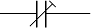
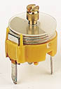
Trimmer capacitors (trimmers) are miniature variable capacitors. They are designed to be mounted directly onto the circuit board and adjusted only when the circuit is built.
A small screwdriver or similar tool is required to adjust trimmers. The process of adjusting them requires patience because the presence of your hand and the tool will slightly change the capacitance of the circuit in the region of the trimmer!
Trimmer capacitors are only available with very small capacitances, normally less than 100pF. It is impossible to reduce their capacitance to zero, so they are usually specified by their minimum and maximum values, for example 2-10pF.
Trimmers are the capacitor equivalent of presets which are miniature variable resistors.
555 Timer
Sub-systems
We can go on to see how RC time constants are employed in two major sub-systems using the 555 Timer I.C.
The 555 timer IC was first introduced around 1971 by the Signetics Corporation
as the SE555/NE555 and was called "The IC Time Machine" and
was also the very first and only commercial timer IC available. It provided
circuit designers with a relatively cheap, stable, and user-friendly integrated
circuit for both monostable and astable applications and more than 30 years on
continues to do so! Since this device was first made commercially available, a
myriad of novel and unique circuits in addition to theses two basic sub-systems
have been also been developed using
555’s and presented in several trade, professional, and hobby publications.
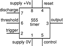
Figure 10.12 IC Pin connection, layout and circuit
symbol 555 Timer
The 555, in fig. 10.12 above, comes in two
packages, either the round metal-can called the 'T' package or the more
familiar 8-pin DIP 'V' package. About 20-years ago the metal-can type was
pretty much the standard (SE/NE types). The 556 timer is a dual 555 version and
comes in a 14-pin DIP package, the 558 is a quad version with four 555's also
in a 14 pin DIP case.
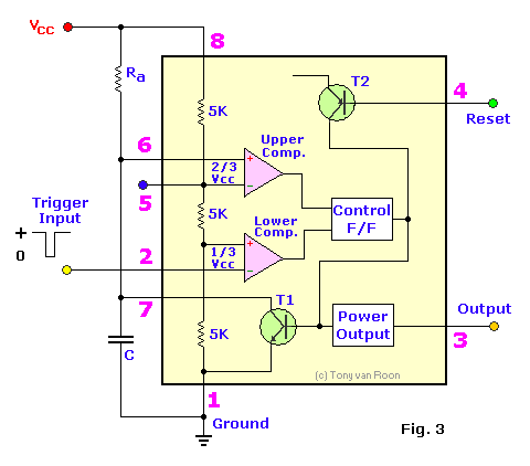
Figure 10.13
Inside the 555 timer.
Inside the
555timer figure 10.13, are the
equivalent of over 20 transistors, 15 resistors, and 2 diodes, depending of the
manufacturer. The figure shows the equivalent circuit, in block diagram,
providing the functions of control, triggering, level sensing or comparison,
discharge, and power output. Some of the more attractive features of the 555
timer are: Supply voltage between 4.5 and 18 volt, supply current 3 to 6 mA,
and a Rise/Fall time of 100 nSec. It can also withstand quite a bit of abuse,
its output can sink or source up to 250mA with up to a 15 volt supply!
The action of the timer is all down to the 2 internal comparators (see chapter 11) so that when the trigger input Pin 2 falls below 1/3rd Vs the device is triggered and the output goes high, like a latching switch. The output can be made to go low again when the threshhold input Pin6 goes above 2/3rds Vs. Thus use of certain RC networks on these input pins allows either single timing pulses (monostable) or continuous pulses (astable) to be generated.
EXAM TOPIC
In more detail
actions at the various pins pertinent to exam knowledge can be summarized as
follows:
Trigger input: when < 1/3 Vs
('active low') this makes the output
high
(+Vs). It monitors the discharging of the timing capacitor in an astable
circuit. It has a high input impedance > 2M![]() .
.
Threshold input:
when > 2/3 Vs ('active high') this makes the
output low (0V)*. It monitors the charging of the timing capacitor in astable
and monostable circuits. It has a high input impedance > 10M![]() .
.
* providing the trigger input is > 1/3 Vs,
otherwise the trigger input will override the threshold input and hold the
output high (+Vs).
Reset input: when less than about 0.7V
('active low') this makes the output low (0V), overriding other inputs. When
not required it should be connected to +Vs. It has an input impedance of about
10k![]() .
.
Control input: this can be used to adjust the threshold voltage which is set internally to be 2/3 Vs. Usually this function is not required and the control input is connected to 0V with a 0.01µF capacitor to eliminate electrical noise. It can be left unconnected if noise is not a problem.
The discharge pin is not an input, but it is
listed here for convenience. It is connected to 0V when the timer output is low
and is used to discharge the timing capacitor in astable and monostable
circuits.
The
astable (EXAM Topic)
The
555 astable, or oscillator, subsystem uses a 555 timer IC to provide an output
signal that constantly switches between high and low states. It is effectively
a pulse subsystem provided good control over the output signal.
The
555 astable is based on the 555 timer IC. The time that the output signal is
high is known as the mark of the
pulse. The time that the output signal is low is known as the space of the pulse.
A mark/space ratio is used to show how much longer the mark time is compared to the space time.
A typical astable circuit diagram feeding a buzzer output device is shown in figure 10.14.
|
|
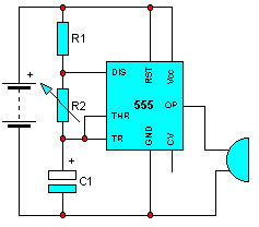
Figure 10.14 555 Astable
In the
basic arrangement is shown above, R1, R2 and C1 are external components whose
values fix the frequency of the stream of continuous square wave pulses
produced automatically at the output (pin 3).
The
period T of the approximate square wave is given by
T = 0.7 (R1+2R2)
C1
Where
again T is in seconds if R is in Megohms and C is in microfarads.
The frequency f = 1/T
The
duty cycle or mark to space ratio is the ratio of the time the
output is on divided by the time the output is off. For a true
square wave this is 1. If you look carefully at the pin out diagram and
circuit you will see that the timing capacitor charges through both R1 and R2
and discharges through R2 only. This means that a rectangular wave is produced
unless R1 is very small in comparison to R2. In practice we cannot make R1 less
than about 1K or the 555 will burn out.
Choosing R1, R2 and C1
|
555 astable frequencies |
|||
|
C1 |
R2 = 10k |
R2 = 100k |
R2 = 1M |
|
0.001µF |
68kHz |
6.8kHz |
680Hz |
|
0.01µF |
6.8kHz |
680Hz |
68Hz |
|
0.1µF |
680Hz |
68Hz |
6.8Hz |
|
1µF |
68Hz |
6.8Hz |
0.68Hz |
|
10µF |
6.8Hz |
0.68Hz |
0.068Hz |
R1 and R2 should
be in the range 1k![]() to 1M
to 1M![]() . It is best to choose C1 first
because capacitors are available in just a few values.
. It is best to choose C1 first
because capacitors are available in just a few values.
- Choose C1 to suit the frequency range you require (use the table as a guide).
- Choose R2 to give the frequency (f) you require. Assume that R1 is much smaller than R2 (so that Tm and Ts are almost equal), then you can use:
|
R2 = |
0.7 |
|
f × C1 |
- Choose R1 to be about a tenth of R2 (1k
 min.) unless you want the mark
time Tm to be significantly longer than the space time Ts.
min.) unless you want the mark
time Tm to be significantly longer than the space time Ts. - If you wish to use a variable resistor it is best to make it R2.
- If R1 is variable it must have a fixed resistor of at least 1k in series
(this is not required for R2 if it is variable).
Astable operation Exam
Topic
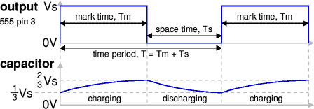
Figure 10.15 Astable timing diagram
With the output high (+Vs) the capacitor C1 is charged by current flowing through R1 and R2. The threshold and trigger inputs monitor the capacitor voltage and when it reaches 2/3Vs (threshold voltage) the output becomes low and the discharge pin is connected to 0V.
The capacitor now discharges with current flowing through R2 into the discharge pin. When the voltage falls to 1/3Vs (trigger voltage) the output becomes high again and the discharge pin is disconnected, allowing the capacitor to start charging again.
This cycle repeats continuously unless the reset input is connected to 0V which forces the output low while reset is 0V.
An astable can be used to provide the clock signal for circuits such as counters.
A low frequency astable (< 10Hz) can be used to flash an LED on and off, higher frequency flashes are too fast to be seen clearly. Driving a loudspeaker or piezo transducer with a low frequency of less than 20Hz will produce a series of 'clicks' (one for each low/high transition) and this can be used to make a simple metronome.
An audio frequency astable
(20Hz to 20kHz) can be used to produce a sound from a loudspeaker or piezo
transducer. The sound is suitable for buzzes and beeps. The natural (resonant)
frequency of most piezo transducers is about 3kHz and this will make them
produce a particularly loud sound.
Duty cycle
The duty cycle of an astable circuit is the proportion of the complete cycle for which the output is high (the mark time). It is usually given as a percentage.
For a standard 555/556 astable circuit the mark time (Tm) or Time High must be greater than the space time (Ts) or Time Low, so the duty cycle must be at least 50%:
|
Duty cycle
= |
Tm |
= |
R1 + R2 |
|
Tm + Ts |
R1 + 2R2 |
Figure 10.16 Astable Duty Cycle.
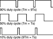
|
|
|
Figure 10.17 555 Astable
circuit with diode across R2 |
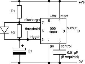
Practical Hint: to achieve a duty cycle of less than 50% a diode can be added in parallel with R2 as shown in the diagram. This bypasses R2 during the charging (mark) part of the cycle so that Tm depends only on R1 and C1:
Tm = 0.7 × R1 × C1 (ignoring 0.7V across diode)
Ts = 0.7 × R2 × C1 (unchanged)
|
Figure 10.18 Duty cycle with diode = |
Tm |
= |
R1 |
|
Tm + Ts |
R1 + R2 |
Use a signal diode such
as 1N4148.
|
THE 555 MONOSTABLE EXAM TOPIC |
|
|
|
|
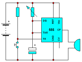
Figure 10.19 555 Monostable
The
555 monostable subsystem figure 10.19 provides an output signal that stays high
for a period of time before returning to low. It is able to provide a range of
time delays up to about 20 minutes with reasonable accuracy. In practice the
timing resistor at the discharge pin should be no higher than 1M and the timing
capacitor at the threshold pin no higher than 1000 microfarads otherwise
leakage currents may dominate and the timing pulse may never reach an end. In
other words the circuit would stay latched on.
The
555 monostable is based on the 555 timer IC. A single pulse is generated by the
monostable when it is triggered by a negative-going input pulse, such as that
produced by the push switch connected to the trigger input. Once triggered the
output remains high for the timed period. This time period can be calculated
using the formula:
T= 1.1 R x C KEY EQUATION
where R is in M ohms and C is in µF
Monostable operation
Exam Topic
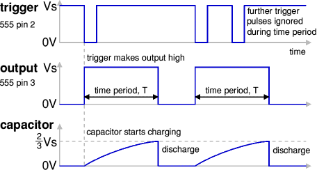
Figure 10.20 Monostable Timing Diagram Exam Topic
The timing period is triggered (started) when the trigger input (555 pin 2) is less than 1/3 Vs, this makes the output high (+Vs) and the capacitor C1 starts to charge through resistor R1. Once the time period has started further trigger pulses are ignored.
The threshold input (555 pin 6) monitors the voltage across C1 and when this reaches 2/3 Vs the time period is over and the output becomes low. At the same time discharge (555 pin 7) is connected to 0V, discharging the capacitor ready for the next trigger.
The reset input (555 pin 4)
overrides all other inputs and the timing may be cancelled at any time by
connecting reset to 0V, this instantly makes the output low and discharges the
capacitor. If the reset function is not required the reset pin should be
connected to +Vs.
|
|
|
Figure 10. 21 Power-on
reset or |
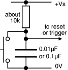
Power-on reset or trigger
It may be useful to ensure that a monostable circuit is reset or triggered automatically when the power supply is connected or switched on. This is achieved by using a capacitor instead of (or in addition to) a push switch as shown in the diagram.
The capacitor takes a short time to charge, briefly holding the input close to 0V when the circuit is switched on. A switch may be connected in parallel with the capacitor if manual operation is also required.
Driving other subsystems (practical
aspects)
For simplicity, the astable and monostable are shown here driving buzzers but it should be remembered they can be allowed to drive any number of other subsystems such as logic or output drivers or other output devices, provided they are corrected interfaced.
Remember this IC. Can sink or source up to 200 mA. This is more than most chips and it is sufficient to supply many output transducers directly, including LEDs (with a resistor in series), low current lamps, piezo transducers, loudspeakers (with a capacitor in series), relay coils (with diode protection) and some motors (with diode protection). The output voltage does not quite reach 0V and +Vs, especially if a large current is flowing.
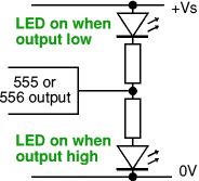 Figure 10.22 Sinking and sourcing
To switch larger currents you can connect a transistor.
The ability to both sink and source current means that two devices can be connected to the output so that one is on when the output is low and the other is on when the output is high. The top diagram shows two LEDs connected in this way..
Loudspeakers
A loudspeaker
(minimum resistance 64![]() ) may be connected to the output of a
555 or 556 astable circuit but a capacitor (about 100µF) must be connected in
series. The output is equivalent to a steady DC of about ½Vs combined with a
square wave AC (audio) signal. The capacitor blocks the DC, but allows the AC
to pass as explained in capacitor coupling.
) may be connected to the output of a
555 or 556 astable circuit but a capacitor (about 100µF) must be connected in
series. The output is equivalent to a steady DC of about ½Vs combined with a
square wave AC (audio) signal. The capacitor blocks the DC, but allows the AC
to pass as explained in capacitor coupling. 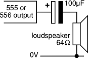 Figure 10.23 Speaker
connection
Figure 10.23 Speaker
connection
Piezo transducers may be connected directly to the output and do not require a capacitor in series.
Relay coils and other inductive loads
Like all ICs, the 555 and 556 must be protected from the brief high voltage 'spike' produced when an inductive load such as a relay coil is switched off. The standard protection diode must be connected 'backwards' across the the relay coil as shown in the diagram.
However, the 555 and 556 require an extra diode connected in series with the coil to ensure that a small 'glitch' cannot be fed back into the IC. Without this extra diode monostable circuits may re-trigger themselves as the coil is switched off! The coil current passes through the extra diode so it must be a 1N4001 or similar rectifier diode capable of passing the current, a signal diode such as a 1N4148 is usually not suitable
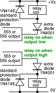 Figure 10.24 Driving Relays
Example
Circuits
The 555 is such a versatile I.C. it has been considered worthy of including a few unusual example circuits which some of you might consider incorporating in some way into course works.
Edge-triggering
|
|
Figure 10.25 Edge-triggering
circuit
|
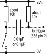
If the trigger input is still less than 1/3 Vs at the end of the time period the output will remain high until the trigger is greater than 1/3 Vs. This situation can occur if the input signal is from an on-off switch or sensor.
The monostable can be made edge triggered, responding only to changes of an input signal, by connecting the trigger signal through a capacitor to the trigger input. The capacitor passes sudden changes (AC) but blocks a constant (DC) signal. For further information please see the page on capacitance. The circuit is 'negative edge triggered' because it responds to a sudden fall in the input signal.
The resistor between the trigger (555 pin 2) and +Vs ensures that the trigger is normally high (+Vs).
555/556 Inverting
Buffer or NOT gate
|
|
|
Figure 10.26 555 as a NOT gate or inverting buffer |
|
|
|
Revision NOT gate
symbol |
The buffer
circuit's input has a very high impedance (about 1M![]() ) so it requires only a few µA, but
the output can sink or source up to 200mA. This enables a high impedance signal
source (such as an LDR) to switch a low impedance output transducer (such as a
lamp).
) so it requires only a few µA, but
the output can sink or source up to 200mA. This enables a high impedance signal
source (such as an LDR) to switch a low impedance output transducer (such as a
lamp).
It is an inverting buffer or NOT gate because the output logic state (low/high) is the inverse of the input state:
- Input low (< 1/3 Vs) makes output high, +Vs
- Input high (> 2/3 Vs) makes output low, 0V
When the input voltage is between 1/3 and 2/3 Vs the output remains in its present state.
Strictly speaking this circuit is more like a Schmitt trigger because its intermediate input region is a deadspace where there is no response, a property called hysteresis, it is like backlash in a mechanical linkage.
If high sensitivity is required
the hysteresis is a problem, but in many circuits it is a helpful property. It
gives the input a high immunity to noise because once the circuit output has
switched high or low the input must change back by at least 1/3 Vs
to make the output switch back, see Figure 10.31 and Schmitt Triggers .
Figure 10.27 Power
Alarm 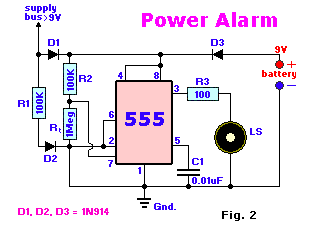
This circuit figure 10.27
can be used as a audible 'Power-out Alarm'. It uses the 555 timer as an
oscillator biased off by the presence of mains line-based DC voltage. When the
line voltage fails, the bias is removed, and the tone will be heard in the
speaker. R1 and C1 provide the DC bias that charges capacitor Ct to over 2/3
voltage, thereby holding the timer output low (as you learned previously).
Diode D1 provides DC bias to the timer-supply pin and, optionally, charges a
rechargeable 9-volt battery across D2. And when the line power fails, DC is furnished
to the timer through D2. A line base voltage is one derived from am mains power
supply, see power supplies.
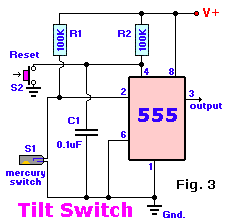
Figure 10.28 Tilt Switch
Actually figure
10.28 is really a alarm circuit, it shows how to use a 555 timer and a small
glass-encapsulated mercury switch to indicate 'tilt'. The switch is mounted in
its normal 'open' position, which allows the timer output to stay low, as
established by C1 on start-up. When S1 is disturbed, causing its contacts to be
bridged by the mercury blob, the 555 latch is set to a high output level where
it will stay even if the switch is returned to its starting position. The high
output can be used to enable an alarm of the visual or the audible type. Switch
S2 will silent the alarm and reset the latch. C1 is a ceramic 0.1uF (=100
nano-Farad) capacitor.
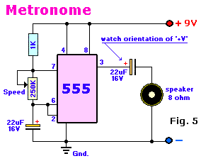
Fig. 10.29 Metronome
Figure 10.28 Essentially shows a variable frequency astable, a Metronome is a device used in the music industry. It indicates the rhythm by a 'toc-toc' sound which speed can be adjusted with the 250K potentiometer. It is very handy if you learning to play music and need to keep the correct rhythm up.
Audio
oscillator
If you want a simple audio oscillator you can experiment with the metronome circuit by reducing the capacitor value. Inserting a Morse key in series with the power lead or speaker lead will give you a Morse code practice oscillator.
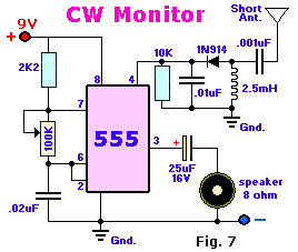
Fig. 10.30 CW Monitor
Any of you
who are licensed radio amateurs may be interested in the circuit shown in
figure 10.30.
This circuit monitors the Morse code 'on-air' via the tuning circuit and diode detector (see radio receivers) hook-up to pin 4 (the reset pin) and the short wire antenna. The 100K potentiometer controls the tone-pitch. The circuit is effectively an astable pulsing in the audio frequency range . When there is no signal present pin 4 is on zero volts and the astable output is permanently reset to zero (no output). When the detector receives a Morse signal a positive voltage is put on the reset pin and the astable pitch is allowed to sound in the speaker. It will therefore sound in sympathy with the incoming signal. You might like to experiment with this circuit as a mobile phone or mobile mast detector as well!
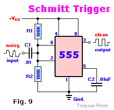
Fig. 10.31 Schmitt
Trigger
Figure 10.31 shows a simple, but effective circuit. It cleans up any noisy input signal in a nice, clean and square output signal. In radio control (R/C) it will clean up noisy servo signals caused by r.f. interference by long servo leads. As long as R1 equals R2, the 555 will automatically be biased for any supply voltage in the 5 to 16 volt range.: It should be noted that there is a 180-degree phase shift, see amplifiers . This circuit also lends itself to condition 60-Hz sine-wave reference signal taken from a 6.3 volt AC transformer before driving a series of binary or divide-by-N counters, see counters. The major advantage is that, unlike a conventional multivibrator type of squarer which divides the input frequency by 2, this method simply squares the 60-Hz sine wave reference signal without division.
The following circuits are examples of how a 555 timer IC assist in combination with another Integrated Circuit. Again, don't be afraid to experiment. Unless you circumvent the min and max parameters of the 555, it is very hard to destroy. Just have fun and learn something doing it.
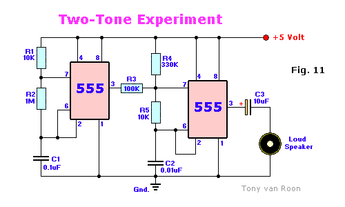
Fig. 10.32
Two-Tones
The purpose of the
experiment shown in figure 10.32 is to wire two 555 timers together
sequentially to create a 2-note tone. If you wish, you can use the dual 556
timer ic.
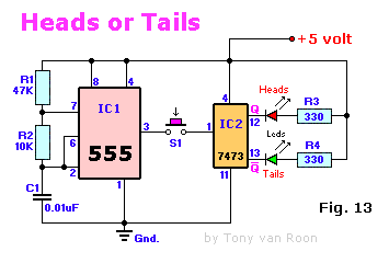
Fig. 10.33 Coin Toss
The electronic 'Heads-or-tails' coin toss
circuit is basically a Yes or No decision maker when you can't
make up your mind yourself. The 555 is wired as a Astable Oscillator, driving
in turn, via pin 3, the 7473
flip-flop, see latches, flip flops, counters etc. When you press S1 it randomly selects the
'Heads' or 'Tails' led. The LEDS flash rate is about 2 KHz (kilo-Hertz), which
is much faster than your eyes can follow, so initially it appears that both LEDS
are 'ON'. As soon as the switch is released only one led will be lit.
CHAPTER 11 OPERATIONAL AMPLIFIERS AND COMPARATORS.
Previously we saw how light and dark sensor circuits could provide high or low outputs that could drive logic sub-systems, similarly for high or low temperature detectors. But what if twilight were applied to our sensor or a medium temperature?
The output voltage would be intermediate between high and low and the logic system would be confused. Comparators are subsystems which enable us to get a good logic signal output from virtually any analogue system input by means of usually one i.c. known as an operational amplifier and a reference voltage input, usually adjustable and obtained form a potential divider sub-system.
We
have seen amplifiers using transistors. (ICs) called operational amplifiers
or op amps often have about 20 or 30 transistors inside them and their inputs
work on a principle which is known as a long tailed pair or current mirror
(this is beyond the scope of an A level text so we will not expand on it here. .
They are called ``operational'' amplifiers, because they can be used to perform
arithmetic operations (addition, subtraction, multiplication) with signals. In
fact, op amps can also be used to integrate (calculate the areas under) and
differentiate (calculate the slopes of) signals.
|
Figure 11.1 A
circuit model of an operational amplifier (op amp) with open loop gain |

A circuit model of an
operational amplifier is shown in Figure 11.1 The output
voltage of the op amp is
linearly proportional to the voltage difference between non inverting and
inverting input terminals ![]() by a factor of the gain
by a factor of the gain![]() . However, the output voltage is
limited to the range
. However, the output voltage is
limited to the range![]() , where
, where ![]() is the supply voltage
specified by the designer of the op amp. The range
is the supply voltage
specified by the designer of the op amp. The range ![]() is often
called the linear region of the amplifier, and when the output swings to
is often
called the linear region of the amplifier, and when the output swings to
![]() or
or ![]() , the op amp is said to be saturated.
An ideal op amp has infinite gain (
, the op amp is said to be saturated.
An ideal op amp has infinite gain (![]() ), infinite input
resistance (
), infinite input
resistance ( ![]() ), and zero output
resistance.
), and zero output
resistance.
Real Op Amps
These have an open loop gain of about 100000 times. Their output voltage is
therfore
given by the following equation:
![]()
This means that for all but a tiny voltage difference (a few microvolts) between the non- inverting and inverting input terminals the output will saturate. However with a real op-amp, saturation occurs at 2 or 3 volts lower than the supply rail voltage.
T Figure 11.2 Op-amp circuit symbol
he usual circuit symbol for an op-amp is:  where:
·
V+: non-inverting input
·
V−: inverting input
·
Vout: output
·
VS+: positive power supply (sometimes also VDD, VCC,
or VCC + )
·
VS−: negative power supply (sometimes also VSS, VEE,
or VCC − )
The power supply pins are (VS+ and VS−)
. The positions of the inverting and non-inverting inputs may be reversed in
diagrams where appropriate; the power supply pins are not commonly reversed.
Connecting an Op Amp
Op amps with 8 pin Dual in Line Packages such as the LM741 should be connected to a breadboard as shown here. The notch is at the top of the op amp, with pins counted counterclockwise from the upper left corner.
Figure
11.3 741 Pin out
The Comparator
This setup is used to determine which input signal is greater. When the inputs are equal, there is no output. When the inverting input is greater, the op amp becomes saturated and output voltage is equal to the voltage of the power supply the op amp is connected to. When the non inverting input is greater, the output voltage is equal to the negative voltage supply, or the negative of the positive supply if connected to ground. Comparators are often used in analog to digital conversions.
Figure 11.4 Comparator
In an absolutely ideal case when the tow inputs are equal there should be no output voltage whatsoever. In practice there may be a tiny voltage known as the offset.
This can be put right using an
offset null control. The recommended circuit for
balancing out the input offset is quite simple, as shown here. The offset null
pins (1 and 5) give direct access to the 1K emitter resistors in the input
stage, and the offset null circuit is simply a 10K potentiometer connected
between them, with its slider connected to the negative power supply. This is
equivalent to putting a 5K resistance in parallel with each of the 1K resistors
inside the IC. The difference is that we can vary the external resistances by
adjusting the potentiometer, until the voltage offset becomes zero.
Comparator
action and circuits; exam topic
An op-amp, used without any limiting feedback, will amplify the
difference between the inputs by the open loop gain. As the open loop gain is
assumed to be very large then even a very small difference between the inputs
will result in the output saturating. The output saturating means that the
output voltage gets as close to the supply voltage as it is able to. For
example, if a standard 741 is used with ±15v power supplies then the output
voltage will either be +13v or -13v unless the inputs are within a few
microvolts of each other
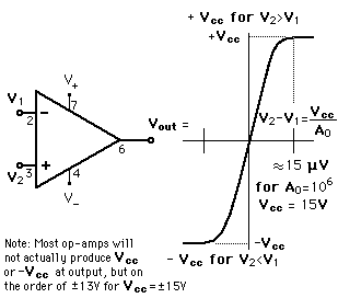 Figure 11.5 Op amp saturation
In effect the op-amp is comparing the two inputs and giving an output that shows which of the inputs is bigger ... hence the op-amp is acting as a comparator
If the Non-inverting input is greater than the Inverting input then the output is positive, if the Inverting input is greater than the Non-inverting input then the output is negative
V+ > V- gives Vout > 0v
V- > V+ gives Vout < 0v
The comparator is useful for detecting when an input goes above or below a certain pre-determined value. In this sense the analogue input voltage is converted into a digital state - either on or off - and so a comparator is a simple 1 bit ADC!! Alternatively, in a simple sense, a comparator is bit like a voting system its output an indicator of whichever input ‘wins’.
Comparator used as a temperature sensor
The circuit diagram shows a comparator used to determine when the temperature goes above or below a threshold temperature
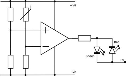
Figure 11.6 Comparator with temperature sensor
- The potential divider forms a voltage reference input sub-system by fixing the non-inverting input at some pre-determined voltage. This "reference" voltage is determined by the values of the resistors used in the potential divider. If a variable reference voltage is required, to set a variable temperature threshold, then a potentiometer can be used instead of the fixed potential divider.
- The inverting input derives a voltage from a potential divider that has a thermistor as one of its resistors and so the voltage at the inverting input varies with temperature. If the temperature increases then the resistance of the thermistor decreases and the voltage at the inverting input increases
- When the temperature is low, the voltage at the non-inverting input is higher than that at the inverting input and the output is positive. Current flows from the 741 (current sourcing) and through the green LED causing it to light
- As the temperature raises, the voltage at the inverting input rises and the instant it is greater than the reference voltage at the non-inverting input, the output becomes negative. Current flows from 0v and into the output of the 741 (current sinking) causing the red LED to light
Comparator used as a light level detector
The circuit below shows a comparator used to detect light level. When the light level passes some pre-determined threshold then the output changes state
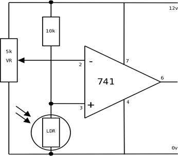
Figure 11.7 Comparator
with light sensor
- A variable resistor is used to set the threshold voltage at the inverting input
- When the light level is high, the resistance of the LDR is low and so the voltage at the non inverting is low, therefore the output is low
- Note that the op-amp uses the 12v and 0v supplies, not the ±12v supplies and so the minimum output voltage is 0v (or 2v in reality)
- When the light level falls, the resistance of the LDR rises and so does the voltage at the non inverting input. This causes the output to go high when the voltage on the non inverting input is greater than the voltage on the inverting input.
- The point at which the output changes state can be set using
the variable resistor
Comparator
used as a range indicator; Practical Topic
The circuit below shows two comparators used to detect when the input voltage is within a given range
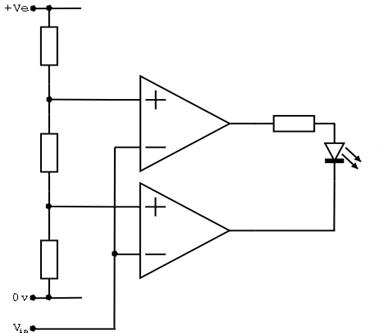
Figure 11.8 Range detector
- When the input voltage is low, the inverting inputs of both op-amps are below the non-inverting inputs. Both outputs are positive and so there is no voltage difference across the LED and it does not light.
- When the input voltage is high, the inverting inputs of both op-amps are above both the non-inverting inputs. Both outputs are negative and again there is no voltage difference across the LED and it does not light.
- When the input voltage is between the two threshold voltages determined by the three resistors in the potential divider chain, the output of the upper op-amp is positive and the output of the lower op-amp is negative and so current flows through the LED and it lights to show that the input voltage is within the range required.
This simple circuit could be the basis of many projects where both upper and lower thresholds are required. If the input voltage is temperature dependent for instance then the output tells you when it is neither too hot nor too cold ... useful for anything from a baby’s room to beer making! Other possibilities exist if the input voltage is dependent on some other factor such as light level or time etc, etc.
Gain bandwidth product and Frequency Response
An op-amp has a very high gain, but only at dc and low
frequencies. As frequency increases, the gain drops off steeply (usually at
usuallyat6 dB per octave or 20dB per decade). Remember that dB = 20*log (Vo/Vi)
so 20 dB is the same as a voltage ratio of 10:1. The output voltage falls by a
factor of ten when the frequency rises by a factor of ten.
If you don’t like the maths just remember that due to the frequency
compensation, the 741's voltage gain falls rapidly with increasing signal
frequency. Typically down to 1000 at 1 kHz, 100 at 10 kHz, and unity at about
1MHz. To make this easy to remember we can say that the 741 has a gain-bandwidth
product of around one million (i.e. 1 MHz as the units of frequency are
Hz).
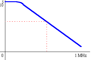 Figure 11. 9 Gain –bandwidth
The gain-bandwidth product is a constant value for any point on the sloping part of the curve shown here. It is typically about 1 MHz for a 741.
It follows from the above that if we had some way of controlling or reducing the gain we might be able to use amplifiers over a wider frequency range. With op-amps this is done using negative feedback. We can then go on to think about how might use op-amps as audio frequency amplifiers and sound mixers.
Op-amps With
Negative Feedback
There are several basic ways in which an op-amp
can be connected using negative feedback to stabilize the gain and increase
frequency response.
The large open-loop gain of an op-amp creates
instability because a small noise voltage on the input can be amplified to a
point where the amplifier is driven out of the linear region.
Open-loop gain varies between devices.
Closed-loop gain is independent of the open-loop
gain.
Closed-Loop voltage gain, Acl
It is the voltage gain of an op-amp with external
feedback.
Gain is controlled by external components.
Figure 11.10 Noninverting Amplifier
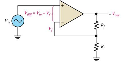
Input signal is applied to the non-inverting input.
The output is applied back to the inverting input through feedback (closed loop) circuit formed by the input resistor Ri and the feedback resistor Rf. This creates a negative feedback.
The two resistors create a voltage divider, which reduces Vout and connects the reduced voltage Vf to the inverting input. The feedback voltage is:
Vf = Ri/(Ri + Rf)Vout
The difference between the input voltage and the feedback voltage is the differential input to the op-amp.
This differential voltage is amplified by the open loop gain, A, to get Vout.
Vout = A(Vin – Vf)
Let B = Ri/(Ri + Rf). Thus Vf = BVout and
Vout = A(Vin – BVout)
Manipulate the expression to get:
Vout = AVin - AolBVout
Vout + ABVout = AolVin
Vout(1 + AB) = AolVin
Overall Gain = Vout/Vin = A/(1 + AB)
Since AolB >> 1, the equation above becomes:
Vout/Vin = Aol/(AolB) = 1/B
Thus the closed loop gain of the noninverting (NI) amplifier is the reciprocal of the attenuation (B) of the feedback circuit (voltage-divider).
A(NI) = Vout/Vin
= 1/B = (Ri + Rf)/Ri
Finally:
A(NI)
= 1 + Rf/Ri
Notice that the closed loop gain is independent of the open-loop gain.
Example
Determine
the gain of the amplifier circuit shown below. The open loop gain of the op-amp
is 150000.
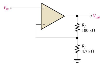
Solution
This
is a non-inverting amplifier op-amp configuration. Therefore, the closed-loop
voltage gain is
A(NI) = 1 + Rf/Ri = 1 + 100 /4.7 = 22.3
Voltage-Follower (VF)
Output voltage of a noninverting amplifier is fed back to the inverting input by a straight connection.
The straight feedback has a gain of 1 (i.e. there is no gain). The closed-loop voltage gain is 1/B, but B = 1. Thus, the A(VF) = 1.
It has very high input impedance and low output impedance.
Figure 11.12 Voltag Follower
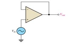
Inverting Amplifier (I)
The input signal is applied through a series input resistor Ri to the inverting input.
The output is fed back through Rf to the same input.
The non-inverting input is grounded.
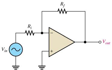
Figure 11.13 Inverting Amplifier with negative Feedback
For finding the gain, let’s assume there is infinite impedance at the input (i.e. between the inverting and non-inverting inputs).
Infinite input impedance implies zero current at the inverting input.
If there is zero current through the input impedance, there is NO voltage drop between the inverting and non-inverting inputs.
Thus, the voltage at the inverting input is zero!
The zero at the inverting input is referred to as virtual earth (ground).
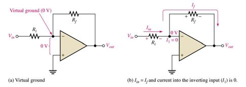
Figure
11.14 Virtual earth
Since there is no current at the inverting input, the current through Ri and the current through Rf are equal:
Iin = If.
The voltage across Ri equals Vin because of virtual ground on the other side of the resistor. Therefore we have that
Iin = Vin/Ri.
Also, the voltage across Rf equals –Vout, because of virtual ground. Therefore:
If = -Vout/Rf
Since If = Iin, we get that:
-Vout/Rf = Vin/Ri
Or, rearranging,
Vout/Vin = -Rf/Ri
So,
A(I) = -Rf/Ri
Thus, the closed loop gain is independent of the op-amp’s internal open-loop gain.
The negative feedback stabilizes the voltage gain.
The negative sign indicates inversion.
Figure 11.15 Op Amp
Summing Amplifier
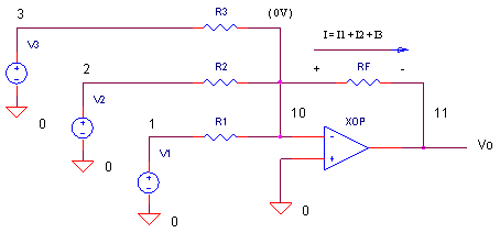
The summing amplifier is a handy circuit enabling you to add several signals together. What are some examples? If you're measuring temperature, you can add a negative offset to make the display read "0" at the freezing point. On a precision amplifier, you may need to add a small voltage to cancel the offset error of the op amp itself. An audio mixer is another good example of adding waveforms (sounds) from different channels (vocals, instruments) together before sending the combined signal to a recorder. It can also be used as a 3-bit D/A Converter.
Just remember that the circuit also inverts the input signals. Not a big deal. If you need the opposite polarity, put an inverting stage with a gain of -1 after the summing amplifier.
Summing Action
The summing action of this circuit is easy to understand if you keep in mind the main "mission" of the op amp. It's a simple one: keep the potential of the negative terminal very close to the positive terminal. In this case, keep the negative terminal close to 0V (virtual ground). Thus the op amp essentially holds one leg of R1, R2 and R3 to a 0V potential. This makes it easy to write the currents in these resistors.
I1 = V1 / R1; I2 = V2 / R2; I3 = V3 / R3
So what's the current I flowing in RF? Using Kirchoff’s Law, we get
I = I1 + I2 + I3
Finally, notice that one leg of RF is also kept at 0V. So the output becomes Vo = -RF x I. Combining these pieces of information, we have a simple description of the amplifier
Vo = - RF (V1 / R1 + V2 / R2 + V3 / R3)
= - (V1 · RF / R1 + V2 · RF / R2 + V3 · RF / R3 )
As you can see, the gain for each input is controlled by its single resistor: K1 = -RF/R1, K2 = -RF/R2 and K3 = -RF/R2.
Thus if RF=R1=R2=R3 then the output would be -( V1+V2+V3)
The Differential Amplifier
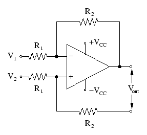
A differential amplifier circuit is shown in Figure
|
|
Uses
- drive
loudspeakers
- amplify
radio frequency energy before feeding to the antenna
- drive DC
motors. Both speed and direction can be controlled.
Source Followers
To
boost current signals form op-amps, source followers are often used.
- The N
Channel FET provides power amplification for the positive part of the AC
input.
- The P
Channel FET provides power amplification for the negative part of the AC input.
- The
voltage gain is 1
- No output
coupling capacitor is needed (avoiding the use of a physically big
component). Single ended (not push pull) amplifiers need a big output
coupling capacitor.
- When
there is no input, neither MOSFET is conducting. This saves energy. Single
ended amplifiers consume power even when there is no input.
- When
there is an AC input, each MOSFET is conducting for only 50% of the time.
Cross Over Distortion
This simple push –pull circuit suffers from cross over distortion.
The red trace is the input signal. The blue trace is the output.
|
|
|


Figure 11.17 Mosfet Push –pull with cross-over
distortion
- Quite a large input voltage is needed to turn
on the FETs, 2 to 4 Volts.
- This has an unwanted side effect. The output
is 2 to 4 volts less than the ideal case.
- A positive potential will turn on the top N
Channel FET.
- A negative potential will turn on the bottom P
Channel FET.
- Small potentials close to zero will turn on
neither FET.
- This causes severe cross over distortion, most
noticeable with quiet music.
- The amplifier works fairly well for potentials
greater than +/- 2 to 4 volts but hardly works at all for lower
potentials.
Bias
the MOSFETs
A
solution to cross-over distortion is to bias the mosfets so they are conducting
all the time.
This diagram shows simple biasing using diodes and resistors. 0.7 Volts
is lost across the diodes so the output will be lower than expected compared
with using ideal components. It is possible to use LEDs. In this case about two
Volts will be lost.

Figure 11.18 Mosfet Push-pull stage with Bias
Adjustable Bias and Quiescent Current
Bias may be refined by additional voltage divider resistors, adjustable
so that both MOSFETS are just on the point of turning on. A small quiescent
current (the current flowing when there is no input signal).
Use Negative Feedback
In addition to biasing, negative feedback
further improves or eliminates cross-over distortion.
- This circuit
uses both biasing and negative feedback to improve performance.
- The LEDs
have two volts across them. This helps to reduce cross over distortion.
This is an unusual way of biasing the MOSFETs but it works.
- The
MOSFETS are included in the feedback path.
- The Op
Amp voltage follower uses a higher power supply voltage. This allows the
MOSFET source follower outputs to swing over a larger range of voltages.
|
Figure 11.19 Mosfet Amplifier with bias and negative feedback |

- This
circuit has a voltage gain of 1 but a much higher power gain (power_out /
power_in).
- The Op
amp output potential will be just right to ensure that Vout = Vin
- Negative
feedback is being used to correct for errors in the output.
- The
operational amplifier is wired up as a voltage follower so Vout should
track Vin exactly.
- Cross
over distortion is minimised.
Push Pull Advantages
- Don't
need a large coupling capacitor between the output and the speaker.
- In other
types of amplifier, this capacitor limits the low frequency response (high
pass filter).
Push Pull Disadvantages
MOSFETs have good high frequency properties. Usually this is an
advantage but it makes it easy to build an oscillator capable of high power
outputs. The oscillations are likely to be outside the range of human hearing
but still able to overheat and destroy speakers, usually the tweeters. Careful
design is needed.
Saturation, Clipping, Limiting
Another
form of distortion is known as saturation distortion or clipping.
This is when the amplifier
cannot produce output voltages that are larger than the power supply voltages. If the input is too big, the
amplifier output will increase until it is nearly equal to the supply voltage.
After that the output voltage cannot rise any more. The red trace below shows
the input. The blue trace shows the amplifier output. The MOSFETs have
saturated. The sine wave input is clipped. The amplifier output is limited (by
the power supply voltage).

RMS Output Power
- The power
supply is 20 Volts.
- An
8Ω speaker is being used.
- Decide
whether to use 20V (ideal) or 18V (real life) in the calculation. If the
exam question does not make it clear which one to use, just say whether
you are doing the ideal or real life calculation. Below, the ideal
calculation is shown.
Vrms = 0.7 x Vpeak
Power = Vrms2 / R
Power = (20 x 0.7)2 / 8
Power = 24.5 Watts
Power audio ICs
As an alternative to discrete components such as op-amps and mosfets
power amplifier ICs can be utilized in radio receivers, hifi’s and AM
modulators
TDA2005 - 20 Watt Class B Amplifier
 The TDA2005 is a class B dual audio power amplifier
specifically designed for car radio applications. Power booster
amplifiers capable of driving very low impedance loads (down to 1.6ohm)
can be designed easily using this device with high current capability
(up to 3.5 A).
The TDA2005 is a class B dual audio power amplifier
specifically designed for car radio applications. Power booster
amplifiers capable of driving very low impedance loads (down to 1.6ohm)
can be designed easily using this device with high current capability
(up to 3.5 A).
TDA1013B - 4W Audio Power Amplifier
 The TDA1013B is an integrated audio amplifier circuit with DC
volume control in a 9 lead single inline plastic package. The wide supply
voltage range makes this circuit ideal for applications in mains and battery
fed devices such as record players and television receivers. This device
requires only a few external components offering stability and performance.
The TDA1013B is an integrated audio amplifier circuit with DC
volume control in a 9 lead single inline plastic package. The wide supply
voltage range makes this circuit ideal for applications in mains and battery
fed devices such as record players and television receivers. This device
requires only a few external components offering stability and performance.
LM386 - Low Voltage Audio Power Amplifier
 LM386 is an audio power amplifier IC
designed for use in low voltage consumer applications. The gain is internally
set to 20, but the addition of an external capacitor resistor between pins 1 -
8 will increase the gain to any value from 20 to 200. The output automatically
biases to one half of the supply voltage. The quiescent power drain is small,
only 24 mW when operating from a 6V supply, making the LM386 ideal for
battery operation.
LM386 is an audio power amplifier IC
designed for use in low voltage consumer applications. The gain is internally
set to 20, but the addition of an external capacitor resistor between pins 1 -
8 will increase the gain to any value from 20 to 200. The output automatically
biases to one half of the supply voltage. The quiescent power drain is small,
only 24 mW when operating from a 6V supply, making the LM386 ideal for
battery operation.
TDA2040 - Hi-Fi 20W Audio Power Amplifier IC
 The TDA2040 is a good quality class AB audio power
amplifier in Pentawatt package. Provides 22W output power (with d = 0.5%) at Vs
= 32V/4ohm. The IC provides high output current and has very low cross-over
and harmonic distortion. The device incorporates a thermal shut-down system
and an efficient short circuit protection system, automatically limiting the
dissipated power to keep the working point of the output transistors within
their safe operating area.
The TDA2040 is a good quality class AB audio power
amplifier in Pentawatt package. Provides 22W output power (with d = 0.5%) at Vs
= 32V/4ohm. The IC provides high output current and has very low cross-over
and harmonic distortion. The device incorporates a thermal shut-down system
and an efficient short circuit protection system, automatically limiting the
dissipated power to keep the working point of the output transistors within
their safe operating area.
TDA2003 - 10W Car Radio Audio Power Amplifier
 The power amplifiers constructed with TDA 2003 need a very
low number of external components. The IC provides high output current
capability (up to 3.5A) with a very low harmonic and cross-over
distortion. A completely safe operation is guaranteed due to the efficient
protection against AC and DC short circuits between all pins and ground, load
dump voltage surge (up to 40V), thermal over-range and fortuitous open ground.
The power amplifiers constructed with TDA 2003 need a very
low number of external components. The IC provides high output current
capability (up to 3.5A) with a very low harmonic and cross-over
distortion. A completely safe operation is guaranteed due to the efficient
protection against AC and DC short circuits between all pins and ground, load
dump voltage surge (up to 40V), thermal over-range and fortuitous open ground.
More power amplifier integrated circuits:
TDA7480 - 10W Class D IC
LM4652 - 170W Class D IC
LM388N - 1.5W AMP IC
LM4755T - 11 Watt Stereo Audio Amp IC
LM1896N - 2Watt Audio Amplifier
TA8251AH - 4ch x 18W Audio Amplifier
TDA7396 - 45Watt/2 Ohm Bridge Car Radio Amplifier
TDA8560Q - 40Watt/2 Ohm Stereo Amplifier IC
TDA1554Q - Power Amplifier IC
KIA6221AH - 30W x 2 (Stereo) Amplifier IC
KIA6216H - 15W BTLX2CH Audio Power Amplifier IC
TDA7240A - 20W Bridge Amplifier IC
Heat sinks
Power
amplifiers generate large amounts of heat due to the internal resistance of
MOSFETS.
Heat sinks are cooling mechanisms used to draw out thermal energy from a variety of electronic components. Without these devices, a wide variety of components would be subject to overheating. The most common heat sink applications are for computer CPU's, microprocessor chips MOSFETS and circuit boards. Readymade heat sinks are implemented for specific solutions, although they are often a part of a system's original design.
The standard materials used to construct a heat sink are aluminum and copper, due to the high conductivity of these metals. Gold plating is also a feature of the better quality heat sinks, as it is used for upping the high transfer of thermal energy. The basic design involves a flat surface placed directly onto the source of heat. Coming out from this is the body of the heat sink, which is often stacked with cooling fins that are used to carry the heat out into the air. The best designs promote thinner fins, so that a greater surface area is then exposed. Thicker fins, however, should be considered for optimal thermal transfer within the heat sink to its cooling fins.
Depending on the device's design, a fan can be applied to create heat sink airflow that benefits the cooling process. If a heat sink is constructed to be passive, then a fan pushing air through it will do little to the overall cooling effect. But regardless of the internal design, heatsink fans are necessary to cool the external air so that heat sinks can function properly.
A variety of measures are taken to decrease a heat sink's thermal resistance, and thereby increase its effectiveness in conducting heat. While the choice of which metal and plating to use is important, other resistance-lowering factors include the smoothness of the heat sink base because the flatter it is, the less resistant it will be. In addition, a special grease or padding can be applied in between the base and the heat source in order to further reduce thermal resistance.
Types of Heatsinks
Heat sinks can be classified in terms of manufacturing methods and their
final form shapes. The most common types of air-cooled heat sinks include:
- Stampings Copper or aluminum sheet
metals are stamped into desired shapes. They are used in traditional air
cooling of electronic components and offer a low cost solution to low
density thermal problems. They are suitable for high volume production,
because advanced tooling with high speed stamping lowers costs. Additional
labour-saving options such as clips and dry interface materials can be factory
applied to help to reduce the board assembly costs.
- Extrusions These are by far the
most common for power amplifiers, and allow the formation of elaborate
two-dimensional shapes capable of dissipating large heat loads. They may
be cut, machined, and options added. Cross-cutting will produce
omni-directional, rectangular pin fin heat sinks, and incorporating
serrated fins improves the performance by approximately 10 to 20%.
Extrusion limits, such as the fin height-to-gap ratio and fin thickness,
usually dictate the flexibility in design options. Typical fin
height-to-gap aspect ratio of up to 6:1 and a minimum fin thickness of
about 1.3mm are attainable with standard extrusion processes.
- Bonded
/ Fabricated Fins Most air cooled heat sinks are convection limited, and the overall
thermal performance of an air cooled heat sink can often be improved
significantly if more surface area can be exposed to the air stream. Such
high performance heat sinks utilise thermally conductive aluminium-filled
epoxy to bond planar fins onto a grooved extrusion base plate. This
process allows for a much greater fin height-to-gap aspect ratio of 20 to
40, greatly increasing the cooling capacity without increasing volume
requirements.
- Castings Sand, lost core and die
casting processes are available with or without vacuum assistance, in
aluminium or (less frequently for audio applications) copper/bronze. This
technology is used in high density pin fin heat sinks which provide
maximum performance when using forced air cooling.
- Folded
Fins
Corrugated sheet metal - either aluminium or copper, increases surface
area and, hence the volumetric performance. The heat sink is then attached
to either a base plate or directly to the heating surface via epoxying or
brazing. It is not suitable for high profile heat sinks, but it allows
high performance heat sinks to be fabricated for specific applications.
Measuring
Heatsink Thermal Resistance
·
The most accurate way to determine the thermal
resistance of an unknown heatsink is to measure it. The exercise is not trivial
though, since you will require a large metal clad resistor having a good flat
bottom surface (or you can use transistors), a contact thermometer (a
conventional alcohol in glass thermometer cannot be used), and a suitable low voltage,
high current power supply. If you have a large number of heatsinks to test it
may be worthwhile to build a dedicated test unit, however this is unlikely for
most home constructors.
·
It is important that the heatsink under test is set
up as closely as possible to the way it will be used. There is no point testing
a sink just lying on the workbench (for example), as the results will be way
off. If a heavy chassis is planned, then attach the heatsink to the chassis or
a reasonable facsimile thereof. Ensure that the heating system is in the best
possible thermal contact with the heatsink. Thermal compound is essential, and
do not use any insulators.
·
The test is based on knowing the voltage and
current you apply to the heatsink heating system (resistor(s) or transistors),
and being able to accurately measure the ambient and heatsink temperatures.
First, apply a relatively low power to the heater system of your choice, and
wait for the heatsink temperature to stabilise - this could take an hour or
more. If the heatsink is too hot or too cold the results will be inaccurate, so
slowly (in steps) increase power until the heatsink is at approximately the
maximum temperature you feel is reasonable (typically around 50-60°C).
·
Measure the ambient temperature and the heatsink
temperature, preferably using the same thermometer. A contact thermometer is
essential for the heatsink (again, use thermal compound). Determine the
temperature difference (temperature rise) between ambient and heatsink.
·
Next, determine the power applied to your heating
system. Thermal resistance may now be established with some very simple maths
...
·
You will use the following terms -
·
Tr - Temperature rise
Ta - Ambient temperature (example 22°C)
Th - Heatsink temperature (example 54°C)
Vh - Voltage to heater (example 12V)
Ih - Current to heater (example 3.5A)
Ph - Power applied to heatsink
Rth - Thermal resistance (in °C/W) so ...
·
Tr = Th - Ta = 54 - 22 = 32°C
Ph = Vh * Ih = 12 * 3.5 = 42W
Rth = Tr / Ph = 32 / 42 = 0.76°C/W
CHAPTER 12: SEQUENTIAL LOGIC
The NAND Gate SR Flip-Flop
The simplest way to make any basic single bit set-reset SR flip-flop is
to connect together a pair of cross-coupled 2-input NAND gates as shown, to
form a Set-Reset Bistable also known as an active LOW SR NAND Gate Latch, so
that there is feedback from each output to one of the other NAND gate inputs.
This device consists of two inputs, one called the Set, S and the other
called the Reset, R with two corresponding outputs Q and its inverse or
complement Q (not-Q) as shown below.
Figure 12.1 The Basic SR Flip-flop
|
|
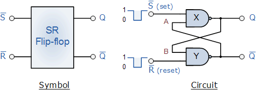
The Set State
Consider the circuit shown above. If the input R is at logic level
"0" (R = 0) and input S is at logic level "1" (S = 1), the
NAND gate Y has at least one of its inputs at logic "0" therefore,
its output Q must be at a logic level "1" (NAND Gate principles).
Output Q is also fed back to input "A" and so both inputs to NAND
gate X are at logic level "1", and therefore its output Q must
be at logic level "0". Again NAND gate principals. If the reset input
R changes state, and goes HIGH to logic "1" with S remaining HIGH
also at logic level "1", NAND gate Y inputs are now R =
"1" and B = "0". Since one of its inputs is still at logic
level "0" the output at Q still remains HIGH at logic level
"1" and there is no change of state. Therefore, the flip-flop circuit
is said to be "Latched" or "Set" with Q = "1" and
Q = "0".
Reset State
In this second stable state, Q is at logic level "0", (not Q =
"0") its inverse output at Q is at logic level "1", (Q =
"1"), and is given by R = "1" and S = "0". As
gate X has one of its inputs at logic "0" its output Q must
equal logic level "1" (again NAND gate principles). Output Q is fed
back to input "B", so both inputs to NAND gate Y are at logic
"1", therefore, Q = "0". If the set input, S now changes
state to logic "1" with input R remaining at logic "1",
output Q still remains LOW at logic level "0" and there is no change
of state. Therefore, the flip-flop circuits "Reset" state has also
been latched and we can define this "set/reset" action in the
following truth table.
Figure 12.2
Truth Table for this Set-Reset Function
|
State |
S |
R |
Q |
Q |
Description |
|
Set |
1 |
0 |
1 |
0 |
Set Q » 1 |
|
1 |
1 |
1 |
0 |
no change |
|
|
Reset |
0 |
1 |
0 |
1 |
Reset Q » 0 |
|
1 |
1 |
0 |
1 |
no change |
|
|
Invalid |
0 |
0 |
0 |
1 |
memory with Q = 0 |
|
0 |
0 |
1 |
0 |
memory with Q = 1 |
It can be seen that when both inputs S = "1" and R = "1"
the outputs Q and Q can be at either logic level "1" or
"0", depending upon the state of inputs S or R BEFORE this input
condition existed. However, input state R = "0" and S = "0"
is an undesirable or invalid condition and must be avoided because this will
give both outputs Q and Q to be at logic level "1" at the same time
and we would normally want Q to be the inverse of Q. However, if the two inputs
are now switched HIGH again after this condition to logic "1", both
the outputs will go LOW resulting in the flip-flop becoming unstable and switch
to an unknown data state based upon the unbalance. This unbalance can cause one
of the outputs to switch faster than the other resulting in the flip-flop
switching to one state or the other which may not be the required state and
data corruption will exist. This unstable condition is known as its Meta-stable
state.
Then, a bistable SR flip-flop or SR latch is activated or set by a logic
"1" applied to its S input and deactivated or reset by a logic
"1" applied to its R. The SR flip-flop is said to be in an
"invalid" condition (Meta-stable) if both the set and reset inputs
are activated simultaneously.
As well as using NAND gates, it is
not also possible to construct simple one-bit SR Flip-flops using two
cross-coupled NOR gates connected in the same configuration. The circuit will
work in a similar way to the D flip-flop
One of the main disadvantages of the basic SR NAND Gate bistable circuit is that the indeterminate
input condition of "SET" = logic "0" and "RESET"
= logic "0" is forbidden. This state will force both outputs to be at
logic "1", over-riding the feedback latching action and whichever
input goes to logic level "1" first will lose control, while the
other input still at logic "0" controls the resulting state of the
latch. In order to prevent this from happening an inverter can be connected
between the "SET" and the "RESET" inputs to produce another
type of flip-flop circuit called a Data Latch, Delay flip-flop, D-type
Bistable or simply a D-type flip-flop as it is more generally
called.
The D flip-flop is by far the most important of the clocked
flip-flops as it ensures that ensures that inputs S and R are never equal to
one at the same time. D-type flip-flops are constructed from a gated SR
flip-flop with an inverter added between the S and the R inputs to allow for a
single D (data) input. This single data input D is used in place of the
"set" signal, and the inverter is used to generate the complementary
"reset" input thereby making a level-sensitive D-type flip-flop from
a level-sensitive RS-latch as now S = D and R = not D as shown.
Figure 12.3 D flip-flop Circuit
|
|
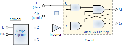
We remember that a simple SR flip-flop requires two inputs, one to
"SET" the output and one to "RESET" the output. By
connecting an inverter (NOT gate) to the SR flip-flop we can "SET"
and "RESET" the flip-flop using just one input as now the two input
signals are complements of each other. This complement avoids the ambiguity
inherent in the SR latch when both inputs are LOW, since that state is no
longer possible.
Thus the single input is called the "DATA" input. If this data
input is HIGH the flip-flop would be "SET" and when it is LOW the
flip-flop would be "RESET". However, this would be rather pointless
since the flip-flop's output would always change on every data input. To avoid
this an additional input called the "CLOCK" or "ENABLE"
input is used to isolate the data input from the flip-flop after the desired
data has been stored. The effect is that D is only copied to the output Q when
the clock is active. This then forms the basis of a D flip-flop.
The D flip-flop will store and output whatever logic level is
applied to its data terminal so long as the clock input is HIGH. This is known as a riding edge triggered
system. Once the clock input goes LOW the "set" and "reset"
inputs of the flip-flop are both held at logic level "1" so it will
not change state and store whatever data was present on its output before the
clock transition occurred. In other words the output is "latched" at
either logic "0" or logic "1". In brief data present at the data input is transferred to the Q output
when the clock goes high and latched there if no further changes occur. Also present on D type flip flops are the
S and R inputs which can function independently
if required. The reset input
is sometimes known as the CLEAR input.
Figure 12.4 Truth Table for the D Flip-flop
|
Clk |
D |
Q |
Q |
Description |
|
↓ » 0 |
X |
Q |
Q |
Memory |
|
↑ » 1 |
0 |
0 |
1 |
Reset Q » 0 |
|
↑ » 1 |
1 |
1 |
0 |
Set Q » 1 |
Note: ↓ and ↑ indicates direction of clock pulse as it is
assumed D flip-flops are edge triggered
ND gate circuit above, except that the inputs are active HIGH and the
invalid condition exists when both its inputs are at logic level "1".
4-bit Data Latch Data
Latches
Another useful application of the Data Latch is to hold or remember the data present on its data input; thereby acting as a single bit memory device and IC's such as the TTL 74LS74 or the CMOS 4042 are available in Quad format for this purpose. By connecting together four, 1-bit data latches so that all their clock terminals are connected at the same time a simple "4-bit" Data latch can be made as shown below.
|
Figure 12.5 4bit data latch |
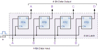
The Shift Register
The Shift Register is another type of sequential logic circuit that is used for the storage or transfer of data in the form of binary numbers and then "shifts" the data out once every clock cycle, hence the name "shift register". It basically consists of several single bit "D-Type Data Latches", one for each bit (0 or 1) connected together in a serial or daisy-chain arrangement so that the output from one data latch becomes the input of the next latch and so on. The data bits may be fed in or out of the register serially, i.e. one after the other from either the left or the right direction, or in parallel, i.e. all together. The number of individual data latches required to make up a single Shift Register is determined by the number of bits to be stored with the most common being 8-bits wide, i.e. eight individual data latches.
The Shift Register is used for data storage or data movement and are used in calculators or computers to store data such as two binary numbers before they are added together, or to convert the data from either a serial to parallel or parallel to serial format. The individual data latches that make up a single shift register are all driven by a common clock (Clk) signal making them synchronous devices. Shift register IC's are generally provided with a clear or reset connection so that they can be "SET" or "RESET" as required.
Generally, shift registers operate in one of four different modes with the basic movement of data through a shift register being:
- Serial-in to Parallel-out (SIPO) - the register is loaded with serial data, one bit at a time, with the stored data being available in parallel form.
- Serial-in to Serial-out (SISO) - the data is shifted serially "IN" and "OUT" of the register, one bit at a time in either a left or right direction under clock control.
- Parallel-in to Serial-out (PISO) - the parallel data is loaded into the register simultaneously and is shifted out of the register serially one bit at a time under clock control.
- Parallel-in to Parallel-out (PIPO) - the parallel data is loaded simultaneously into the register, and transferred together to their respective outputs by the same clock pulse.
The effect of data movement from left to right through a shift register can be presented graphically as:
Figure 12.6 Data movement in a Shift
Register
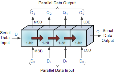
Also, the directional movement of the data through a shift register can be either to the left, (left shifting) to the right, (right shifting) left-in but right-out, (rotation) or both left and right shifting within the same register thereby making it bidirectional. In this tutorial it is assumed that all the data shifts to the right, (right shifting).
Serial-in to
Parallel-out (SIPO)
Figure 12.7 4-bit
Serial-in to Parallel-out Shift Register
|
|
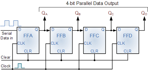
The operation is as follows. Let’s assume that all the flip-flops (FFA to FFD)
have just been RESET (CLEAR input) and that all the outputs QA to QD
are at logic level "0" i.e. no parallel data output. If a logic
"1" is connected to the DATA input pin of FFA then on the first clock
pulse the output of FFA and therefore the resulting QA will be set
HIGH to logic "1" with all the other outputs still remaining LOW at
logic "0". Assume now that the DATA input pin of FFA has returned LOW
again to logic "0" giving us one data pulse or 0-1-0.
The second clock pulse will change the output of FFA to logic "0" and the output of FFB and QB HIGH to logic "1" as its input D has the logic "1" level on it from QA. The logic "1" has now moved or been "shifted" one place along the register to the right as it is now at QA. When the third clock pulse arrives this logic "1" value moves to the output of FFC (QC) and so on until the arrival of the fifth clock pulse which sets all the outputs QA to QD back again to logic level "0" because the input to FFA has remained constant at logic level "0".
The effect of each clock pulse is to shift the data contents of each stage one place to the right, and this is shown in the following table until the complete data value of 0-0-0-1 is stored in the register. This data value can now be read directly from the outputs of QA to QD. Then the data has been converted from a serial data input signal to a parallel data output. The truth table and following waveforms show the propagation of the logic "1" through the register from left to right as follows.
Figure 12.8 Basic
Movement of Data through a Shift Register
|
Clock Pulse No |
QA |
QB |
QC |
QD |
|
0 |
0 |
0 |
0 |
0 |
|
1 |
1 |
0 |
0 |
0 |
|
2 |
0 |
1 |
0 |
0 |
|
3 |
0 |
0 |
1 |
0 |
|
4 |
0 |
0 |
0 |
1 |
|
5 |
0 |
0 |
0 |
0 |
|
|
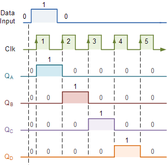
Figure
12.9 4 Bit Shift Register Timing Diagram
Note that after the fourth clock pulse has ended the 4-bits of data (0-0-0-1)
are stored in the register and will remain there provided clocking of the
register has stopped. In practice the input data to the register may consist of
various combinations of logic "1" and "0". Commonly
available SIPO IC's include the standard 8-bit 74LS164 or the 74LS594.
The Ring Counter
Above we saw that if we apply a serial data signal to the input of a serial-in to serial-out shift register, the same sequence of data will exit from the last flip-flip in the register chain after a preset number of clock cycles thereby acting as a sort of time delay circuit to the original signal. What if we were to connect the output of this shift register back to its input so that the output from the last flip-flop, QD becomes the input of the first flip-flop, DA. We would then have a closed loop circuit that "recirculates" the DATA around a continuous loop for every state of its sequence, and this is the principal operation of a Ring Counter. Then by looping the output back to the input, we can convert a standard shift register into a ring counter. Consider the circuit below.
Figure
12.10 4-bit Ring Counter
|
|
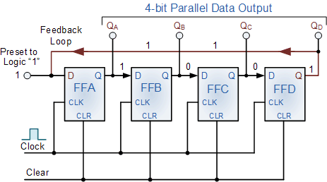
The synchronous Ring Counter example above is preset so that
exactly one data bit in the register is set to logic "1" with all the
other bits reset to "0". To achieve this, a "CLEAR" signal
is firstly applied to all the flip-flops together in order to "RESET"
their outputs to a logic "0" level and then a "PRESET"
pulse is applied to the input of the first flip-flop (FFA)
before the clock pulses are applied. This then places a single logic
"1" value into the circuit of the ring counter . On each successive
clock pulse, the counter circulates the same data bit between the four
flip-flops over and over again around the "ring" every fourth clock
cycle. But in order to cycle the data correctly around the counter we must
first "load" the counter with a suitable data pattern as all logic
"0"'s or all logic "1"'s outputted at each clock cycle
would make the ring counter invalid.
This type of data movement is called "rotation", and like the previous shift register, the effect of the movement of the data bit from left to right through a ring counter can be presented graphically as follows along with its timing diagram:
Figure
12.13 Rotational Movement of a Ring
Counter
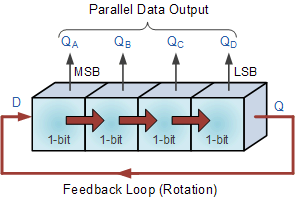
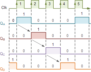
Since the ring counter example shown above has four distinct states, it is also
known as a "modulo-4" or "mod-4" counter with each
flip-flop output having a frequency value equal to one-fourth or a quarter
(1/4) that of the main clock frequency.
The "MODULO" or "MODULUS" of a counter is the number of states the counter counts or sequences through before repeating itself and a ring counter can be made to output any modulo number. A "mod-n" ring counter will require "n" number of flip-flops connected together to circulate a single data bit providing "n" different output states. For example, a mod-8 ring counter requires eight flip-flops and a mod-16 ring counter would require sixteen flip-flops. However, as in our example above, only four of the possible sixteen states are used, making ring counters very inefficient in terms of their output state usage.
Johnson Ring Counter
The Johnson Ring Counter or "Twisted Ring Counters", is another shift register with feedback exactly the same as the standard Ring Counter above, except that this time the inverted output Q of the last flip-flop is now connected back to the input D of the first flip-flop as shown below. The main advantage of this type of ring counter is that it only needs half the number of flip-flops compared to the standard ring counter in other words, it has a halved modulo number. So an "n-stage" Johnson counter will circulate a single data bit giving sequence of 2n different states and can therefore be considered as a "mod-2n counter".
Figure
12.14 4-bit Johnson Ring Counter
|
|
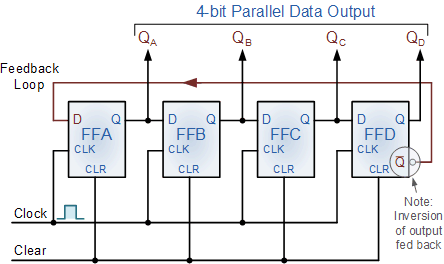
This inversion of Q before it is fed back to input D causes the counter to "count" in a different way.
Instead of counting through a fixed set of patterns like the normal ring
counter such as for a 4-bit counter, "0001"(1), "0010"(2),
"0100"(4), "1000"(8) and repeat, the Johnson counter counts
up and then down as the initial logic "1" passes through it to the
right replacing the preceding logic "0". A 4-bit Johnson ring counter
passes blocks of four logic "0" and then four logic "1"
thereby producing an 8-bit pattern. As the inverted output Q
is connected to the input D this 8-bit pattern
continually repeats. For example, "1000", "1100",
"1110", "1111", "0111", "0011",
"0001", "0000" and this is demonstrated in the following
table below.
Figure
12.15 Truth Table for a 4-bit Johnson Ring Counter
|
Clock Pulse No |
FFA |
FFB |
FFC |
FFD |
|
0 |
0 |
0 |
0 |
0 |
|
1 |
1 |
0 |
0 |
0 |
|
2 |
1 |
1 |
0 |
0 |
|
3 |
1 |
1 |
1 |
0 |
|
4 |
1 |
1 |
1 |
1 |
|
5 |
0 |
1 |
1 |
1 |
|
6 |
0 |
0 |
1 |
1 |
|
7 |
0 |
0 |
0 |
1 |
As well as counting or rotating data around a continuous loop, ring counters
can also be used to detect or recognise various patterns or number values
within a set of data. By connecting simple logic gates such as the AND or
the OR
gates to the outputs of the flip-flops the circuit can be made to detect a set
number or value. Standard 2, 3 or 4-stage Johnson ring counters can also be
used to divide the frequency of the clock signal by varying their feedback
connections and divide-by-3 or divide-by-5 outputs are also available.
A 3-stage Johnson Ring Counter can also be used as a 3-phase, 120 degree phase shift square wave generator by connecting to the data outputs at A, B and NOT-B. The standard 5-stage Johnson counter such as the commonly available CD4017 is generally used as a synchronous decade counter/divider circuit. The smaller 2-stage circuit is also called a "Quadrature" (sine/cosine) Oscillator/Generator and is used to produce four individual outputs that are each "phase shifted" by 90 degrees with respect to each other, and this is shown below.
Figure
12.15 2-bit Quadrature Generator and timing diagram
|
|
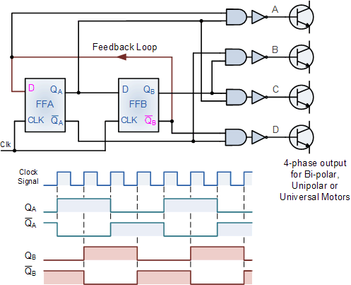
|
Output |
A |
B |
C |
D |
|
QA+QB |
1 |
0 |
0 |
0 |
|
QA+QB |
0 |
1 |
0 |
0 |
|
QA+QB |
0 |
0 |
1 |
0 |
|
QA+QB |
0 |
0 |
0 |
1 |
|
2-bit Quadrature Oscillator, Count Sequence |
||||
As the four outputs, A to D are
phase shifted by 90 degrees with regards to each other, they can be used with
additional circuitry, to drive a 2-phase full-step stepper motor for position
control or the ability to rotate a motor to a particular location as shown
below.
Figure
12.16 Stepper Motor Control
|
|
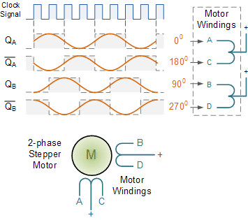
2-phase (unipolar) Full-Step Stepper Motor Circuit
The speed of rotation of the Stepper Motor will depend mainly upon the clock frequency and additional circuitry would be require to drive the "power" requirements of the motor. As this section is only intended to give the reader a basic understanding of Johnson Ring Counters and its applications, other good websites explain in more detail the types and drive requirements of stepper motors.
Johnson Ring Counters are available in standard TTL or CMOS IC form, such as the CD4017 5-Stage, decade Johnson ring counter with 10 active HIGH decoded outputs or the CD4022 4-stage, divide-by-8 Johnson counter with 8 active HIGH decoded outputs.
Frequency Division and Binary
Counters
One main use of a D flip-flop is as a Frequency Divider. If the Q output on a D-type flip-flop is connected directly to the D input giving the device closed loop "feedback", successive clock pulses will make the bistable "toggle" once every two clock cycles.
In the counters tutorials we saw how the Data Latch can be used as a "Binary Divider", or a "Frequency Divider" to produce a "divide-by-2" counter circuit, that is, the output has half the frequency of the clock pulses. By placing a feedback loop around the D flip-flop another type of flip-flop circuit can be constructed called a T-type flip-flop or more commonly a T-type bistable, that can be used as a divide-by-two circuit in binary counters as shown below.
Figure
12.17 Divide-by-2 Counter
|
|
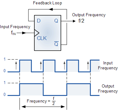
It can be seen from the frequency waveforms above, that by "feeding back" the output from Q to the input terminal D, the output pulses at Q have a frequency that are exactly one half (f/2) that of the input clock frequency, (Fin). In other words the circuit produces frequency division as it now divides the input frequency by a factor of two (an octave) as Q = 1 once every two clock cycles.
Toggle Flip-Flop
Another type of device that can be used for frequency division is the
T-type or Toggle flip-flop. With a slight modification to a standard JK
flip-flop, we can construct a new type of flip-flop called a Toggle
flip-flop were the two inputs J and k of a JK flip-flop are connected
together resulting in a device with only two inputs, the "Toggle"
input itself and the controlling "Clock" input. The name "Toggle
flip-flop" indicates the fact that the flip-flop has the ability to toggle
between its two states, the "toggle state" and the "memory
state". Since there are only two states, a T-type flip-flop is ideal for
use in frequency division and counter design.
Similarly a D-type flip flop will work without the need for external
connection other than Q BAR to Data input.
Binary ripple counters can thus be built using "Toggle" or
"T-type flip-flops" by connecting the output of one to the clock
input of the next, or by using D-TYPE flip flops. Such flip-flops are ideal for building ripple
counters as it toggles from one state to the next, (HIGH to LOW or LOW to HIGH)
at every clock cycle so simple frequency divider and ripple counter circuits
can easily be constructed using standard integrated circuits.
If we connect together in series, two T-type flip-flops the initial
input frequency will be "divided-by-two" by the first flip-flop ( f÷2
) and then "divided-by-two" again by the second flip-flop ( f÷2 )÷2,
giving an output frequency which has effectively been divided four times, then
its output frequency becomes one quarter value (25%) of the original clock frequency,
( f÷4 ). Each time we add another toggle or "T-type" flip-flop the
output clock frequency is halved or divided-by-2 again and so on, giving an
output frequency of 2n where "n" is the number of
flip-flops used in the sequence.
Then the Toggle or T-type flip-flop is an edge triggered divide-by-2
device based upon the standard JK-type flip flop and which is triggered on the
rising edge of the clock signal. The result is that each bit moves right by one
flip-flop. All the flip-flops can be asynchronously reset and can be triggered
to switch on either the leading or trailing edge of the input clock signal
making it ideal for Frequency Division.
Figure 12.18 Frequency Division using Toggle
Flip-flops
|
|

This type of counter circuit used for frequency division is commonly known as
an Asynchronous 3-bit Binary Counter as the output on QA to QC, which is
3 bits wide, is a binary count from 0 to 7 for each clock pulse. In an
asynchronous counter, the clock is applied only to the first stage with the
output of one flip-flop stage providing the clocking signal for the next
flip-flop stage and subsequent stages derive the clock from the previous stage
with the clock pulse being halved by each stage.
This arrangement is commonly known as Asynchronous that is each clocking
event occurs independently as all the bits in the counter do not all change at
the same time, as the counter counts sequentially in an upwards direction from
0 to 7. This type of counter is also known as an "up" or
"forward" counter (CTU) or a "3-bit Asynchronous up
Counter". The three-bit asynchronous counter shown is typical and uses
flip-flops in the toggle mode. Asynchronous "Down" counters (CTD)
are also available.
Figure 12.19 Truth Table for a 3-bit Asynchronous up Counter
|
Clock |
Output bit Pattern |
||
|
QC |
QB |
QA |
|
|
0 |
0 |
0 |
0 |
|
1 |
0 |
0 |
1 |
|
2 |
0 |
1 |
0 |
|
3 |
0 |
1 |
1 |
|
4 |
1 |
0 |
0 |
|
5 |
1 |
0 |
1 |
|
6 |
1 |
1 |
0 |
|
7 |
1 |
1 |
1 |
Then by cascading together D-type or Toggle Flip-Flops we can produce
divide-by-2, 4, 8 etc, asynchronous counter circuits which divide the clock
frequency 2, 4 or 8 times.
Counters
A counter is a specialized register or pattern generator that produces a
specified output pattern or sequence of binary values (or states) upon the
application of an input pulse called the "Clock". The clock is
actually used for data in these applications. Typically, counters are logic
circuits than can increment or decrement a count by one but when used as
asynchronous divide-by-n counters they are able to divide these input pulses
producing a clock division signal.
Counters are formed by connecting flip-flops together and any number of
flip-flops can be connected or "cascaded" together to form a
"divide-by-n" binary counter where "n" is the number of
counter stages used and which is called the Modulus. The modulus or
simply "MOD" of a counter is the number of output states the counter
goes through before returning itself back to zero, i.e., one complete cycle. A
counter with three flip-flops like the circuit above will count from decimal
zero 0 to 7 i.e., 2n-1. It has eight different output states (2n) representing the decimal numbers 0 to 7 and
is called a Modulo-8 or MOD-8 counter. A counter with four
flip-flops will count from 0 to 15 and is therefore called a Modulo-16
counter and so on.
An example of this is given as.
- 3-bit
Binary Counter = 23 = 8 (modulo-8 or MOD-8)
-
- 4-bit
Binary Counter = 24 = 16 (modulo-16 or MOD-16)
-
- 8-bit
Binary Counter = 28 = 256 (modulo-256 or MOD-256)
The Modulo number can be increased by adding more flip-flops to the
counter and cascading is a method of achieving higher modulus counters. Then
the modulo or MOD number can simply be written as: MOD number = 2n
Figure 12.20 4-bit Modulo-16 Counter and timing diagram
|
|
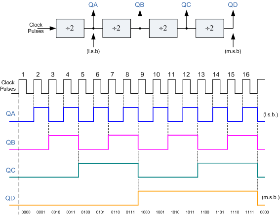
Multi-bit asynchronous counters connected in this manner are also called "Ripple
Counters" or ripple dividers because the change of state at each stage
appears to "ripple" itself through the counter from the LSB output to
its MSB output connection. Ripple counters are available in standard IC form,
from the 74LS393 Dual 4-bit counter to the 74HC4060, which is a 14-bit ripple
counter with its own built in clock oscillator and produce excellent frequency
division of the fundamental frequency.
Frequency
Division Summary
For frequency division,
toggle mode flip-flops are used in a chain as a divide by two counter. One
flip-flop will divide the clock, ƒin by 2, two flip-flops will divide ƒin by 4
(and so on). One benefit of using toggle flip-flops for frequency division is
that the output at any point has an exact 50% duty cycle.
The final output clock signal
will have a frequency value equal to the input clock frequency divided by the
MOD number of the counter. Such circuits are known as "divide-by-n" counters.
Counters can be formed by connecting individual flip-flops together and are
classified according to the way they are clocked. In Asynchronous counters,
(ripple counter) the first flip-flop is clocked by the external clock pulse and
then each successive flip-flop is clocked by the output of the preceding
flip-flop. In Synchronous counters, the clock input is connected to all
of the flip-flop so that they are clocked simultaneously.
Asynchronous Counter
and Decade Counters
In the previous tutorial we saw that an Asynchronous counter can have 2n-1 possible counting states e.g. MOD-16 for a 4-bit counter, (0-15) making it ideal for use in Frequency Division. But it is also possible to use the basic asynchronous counter to construct special counters with counting states less than their maximum output number by forcing the counter to reset itself to zero at a pre-determined value producing a type of asynchronous counter that has truncated sequences. Then an n-bit counter that counts up to its maximum modulus (2n) is called a full sequence counter and a n-bit counter whose modulus is less than the maximum possible is called a truncated counter.
But why would we want to create an asynchronous truncated counter that is not a MOD-4, MOD-8, or some other modulus that is equal to the power of two. The answer is that we can by using combinational logic to take advantage of the asynchronous inputs on the flip-flop. If we take the modulo-16 asynchronous counter and modified it with additional logic gates it can be made to give a decade (divide-by-10) counter output for use in standard decimal counting and arithmetic circuits.
Such counters are generally referred to as Decade Counters. A decade counter requires resetting to zero when the output count reaches the decimal value of 10, ie. when DCBA = 1010 and to do this we need to feed this condition back to the reset input. A counter with a count sequence from binary "0000" (BCD = "0") through to "1001" (BCD = "9") is generally referred to as a BCD binary-coded-decimal counter because its ten state sequence is that of a BCD code but binary decade counters are more common.
Figure 12.21 Asynchronous
Decade Counter
|
|
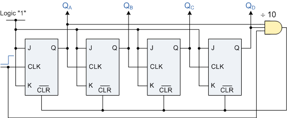
This type of asynchronous counter counts upwards on each leading edge of the input clock signal starting from "0000" until it reaches an output "1010" (decimal 10). Both outputs QB and QD are now equal to logic "1" and the output from the NAND gate changes state from logic "1" to a logic "0" level and whose output is also connected to the CLEAR (CLR) inputs of all the J-K Flip-flops. This causes all of the Q outputs to be reset back to binary "0000" on the count of 10. Once QB and QD are both equal to logic "0" the output of the NAND gate returns back to a logic level "1" and the counter restarts again from "0000". We now have a decade or Modulo-10 counter.
Figure 12.22 Decade
Counter Truth Table
|
Clock |
Output bit Pattern |
Decimal |
|||
|
QD |
QC |
QB |
QA |
||
|
1 |
0 |
0 |
0 |
0 |
0 |
|
2 |
0 |
0 |
0 |
1 |
1 |
|
3 |
0 |
0 |
1 |
0 |
2 |
|
4 |
0 |
0 |
1 |
1 |
3 |
|
5 |
0 |
1 |
0 |
0 |
4 |
|
6 |
0 |
1 |
0 |
1 |
5 |
|
7 |
0 |
1 |
1 |
0 |
6 |
|
8 |
0 |
1 |
1 |
1 |
7 |
|
9 |
1 |
0 |
0 |
0 |
8 |
|
10 |
1 |
0 |
0 |
1 |
9 |
|
11 |
Counter Resets its Outputs back to Zero |
||||
Figure 12.23 Decade
Counter Timing Diagram
|
|
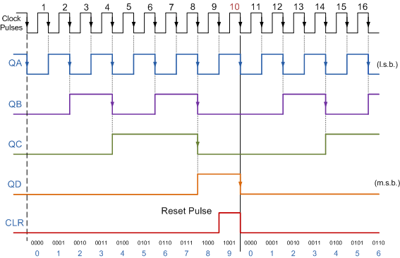
Using the same idea of truncating counter output sequences, the above circuit
could easily be adapted to other counting cycles be simply changing the
connections to the AND gate. For example, a scale-of-twelve (modulo-12) can
easily be made by simply taking the inputs to the AND gate from the outputs at
"QC" and "QD", noting that the binary equivalent of 12 is
"1100" and that output "QA" is the least significant bit
(LSB). Since the maximum modulus that can be implemented with n flip-flops is
2n, this means that when you are designing truncated counters you should
determine the lowest power of two that is greater than or equal to your desired
modulus. For example, lets say you wish to count from 0 to 39, or mod-40. Then
the highest number of flip-flops required would be six, n = 6 giving a maximum
MOD of 64 as five flip-flops would only equal MOD-32. Figure
12.24 Example divider circuit
Then suppose we wanted to
build a "divide-by-128" counter for frequency division we would need
to cascade 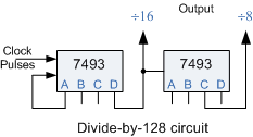 seven flip-flops since 128 = 27. Using dual flip-flops
such as the 74LS74 we would still need four IC's to complete the circuit. One
easy alternative method would be to use two TTL 7493's as 4-bit ripple
counter/dividers. Since 128 = 16 x 8, one 7493 could be configured as a
"divide-by-16" counter and the other as a "divide-by-8"
counter. The two IC's would be cascaded together to form a "divide-by-128"
frequency divider as shown.
seven flip-flops since 128 = 27. Using dual flip-flops
such as the 74LS74 we would still need four IC's to complete the circuit. One
easy alternative method would be to use two TTL 7493's as 4-bit ripple
counter/dividers. Since 128 = 16 x 8, one 7493 could be configured as a
"divide-by-16" counter and the other as a "divide-by-8"
counter. The two IC's would be cascaded together to form a "divide-by-128"
frequency divider as shown.
Of course standard IC asynchronous counters are available such as the TTL 74LS90 programmable ripple counter/divider which can be configured as a divide-by-2, divide-by-5 or any combination of both. The 74LS390 is a very flexible dual decade driver IC with a large number of "divide-by" combinations available ranging form divide-by-2, 4, 5, 10, 20, 25, 50, and 100.
Frequency Dividers
This ability of the ripple counter to truncate sequences to produce a "divide-by-n" output means that counters and especially ripple counters, can be used as frequency dividers to reduce a high clock frequency down to a more usable value for use in digital clocks and timing applications. For example, assume we require an accurate 1Hz timing signal to operate a digital clock. We could quite easily produce a 1Hz square wave signal from a standard 555 timer chip but the manufacturers data sheet tells us that it has a typical 1-2% timing error depending upon the manufacturer, and at low frequencies a 2% error at 1Hz is not good. However the data sheet also tells us that the maximum operating frequency of the 555 timer is about 300kHz and a 2% error at this high frequency would be acceptable. So by choosing a higher timing frequency of say 262.144kHz and an 18-bit ripple (Modulo-18) counter we can make a precision 1Hz timing signal as shown below.
Figure 12.25 Simple
1Hz timing signal using an 18-bit ripple counter/divider.
|
|
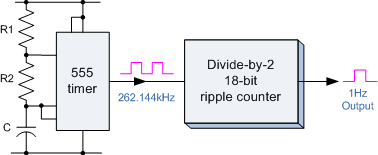
This is of course a very simple example of how to produce accurate frequencies, but by using high frequency crystal oscillators and multi-bit frequency dividers, precision frequency generators can be produced for a range of applications ranging from clocks or watches to event timing and even electronic piano/synthesizer music applications.
The main disadvantages with asynchronous counters are that there is a small delay between the arrival of the clock pulse and its output due to the internal circuitry of the gate. In asynchronous circuits this delay is called the Propagation Delay (giving the asynchronous ripple counter the nickname of propagation counter) and in some cases can produce false output counts. In large bit ripple counter circuits the delay of all the separate stages are added together to give a summed delay at the end of the chain which is why asynchronous counters are generally not used for in high frequency counting circuits were large numbers of bits are involved.
Also, the outputs from the counter do not have a fixed time relationship with each other and do not occur at the same time due to their clocking sequence. Then, the more flip-flops that are added to an asynchronous counter chain the lower the maximum operating frequency becomes. To overcome the problem of propagation delay Synchronous Counters were developed.
Then to summarise:
- Asynchronous Counters can be made from Toggle or D-type
flip-flops.
- They
are called asynchronous counters because the clock input of the flip-flops
are not all driven by the same clock signal.
- Each
output in the chain depends on a change in state from the previous
flip-flops output.
- Asynchronous
counters are sometimes called ripple counters because the data appears to
"ripple" from the output of one flip-flop to the input of the
next.
- They
can be implemented using "divide-by-n" circuits.
- Truncated
counters can produce any modulus number count.
Disadvantages of Asynchronous Counters:
- An
extra "re-synchronizing" output flip-flop may be required.
- To
count a truncated sequence not equal to 2n, extra feedback logic is
required.
- Counting
a large number of bits, propagation delay by successive stages may become
undesirably large.
- This
delay gives them the nickname of "Propagation Counters".
- Counting
errors at high clocking frequencies.
- Synchronous
Counters are faster using the same clock signal for all flip-flops.
CHAPTER 13 AUDIO FILTERS
Audio
filters are essential parts of many modern radio communication system both in
transmitters and receivers.
Low Pass Filter Introduction
Basically, an electrical filter is a circuit that can be designed to modify, reshape or reject all unwanted frequencies of an electrical signal and accept or pass only those signals wanted by the circuits designer. In other words they "filter-out" unwanted signals and an ideal filter will separate and pass sinusoidal input signals based upon their frequency. In low frequency applications (up to 100kHz), passive filters are usually made from simple RC (Resistor-Capacitor) networks while higher frequency filters (above 100kHz) are usually made from RLC (Resistor-Inductor-Capacitor) components. Passive filters are made up of passive components such as resistors, capacitors and inductors and have no amplifying elements (transistors, op-amps, etc) so have no signal gain, therefore their output level is always less than the input.
Filters are named according to the frequency of signals they allow to pass through them. There are Low-pass filters that allow only low frequency signals to pass, High-pass filters that allow only high frequency signals to pass through, and Band-pass filters that allow signals falling within a certain frequency range to pass through. Simple First-order passive filters (1st order) can be made by connecting together a single resistor and a single capacitor in series across an input signal, (Vin) with the output of the filter, (Vout) taken from the junction of these two components. Depending on which way around we connect the resistor and the capacitor with regards to the output signal determines the type of filter construction resulting in either a Low Pass Filter or a High Pass Filter.
As the function of any filter is to allow signals of a given band of frequencies to pass unaltered while attenuating or weakening all other unwanted frequencies, we can define the amplitude response characteristics of an ideal filter by using an ideal frequency response curve of the four basic filter types as shown.
Figure 13.1
Ideal Filter Response Curves
|
|
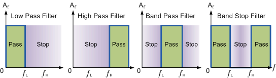
Filters can be divided into two distinct types: active filters and passive
filters. Active filters contain amplifying devices to increase signal strength
while passive do not contain amplifying devices to strengthen the signal. As
there are two passive components within a passive filter design the output
signal has smaller amplitude than its corresponding input signal, therefore
passive RC filters attenuate the signal and have a gain of less than one,
(unity).
A Low Pass Filter can be a combination of capacitance; inductance or resistance intended to produce high attenuation above a specified frequency and little or no attenuation below that frequency. The frequency at which the transition occurs is called the "cutoff" frequency. The simplest low pass filters consist of a resistor and capacitor but more sophisticated low pass filters have a combination of series inductors and parallel capacitors. In this tutorial we will look at the simplest type, a passive two component RC low pass filter.
The Low Pass Filter
A simple passive Low Pass Filter or LPF, can be easily made by connecting together in series a single Resistor with a single Capacitor as shown below. In this type of filter arrangement the input signal (Vin) is applied to the series combination (both the Resistor and Capacitor together) but the output signal (Vout) is taken across the capacitor only. This type of filter is known generally as a "first-order filter" or "one-pole filter", why first-order or single-pole? This is because it has only "one" reactive component in the circuit, the capacitor.
Figure 13.2
Low Pass Filter Circuit
|
|
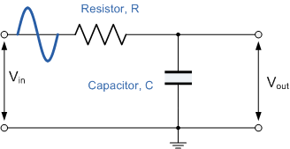
The reactance of a capacitor varies inversely with frequency, while the value of the resistor remains constant as the frequency changes. At low frequencies the capacitive reactance, (Xc) of the capacitor will be very large compared to the resistive value of the resistor, R and as a result the voltage across the capacitor, Vc will also be large while the voltage drop across the resistor, Vr will be much lower. At high frequencies the reverse is true with Vc being small and Vr being large.
While the circuit above is that of an RC Low Pass Filter circuit, it can also be classed as a frequency variable potential divider circuit similar to the one we looked at in the section on Resistors. Then we used the following equation to calculate the output voltage for two single resistors connected in series.
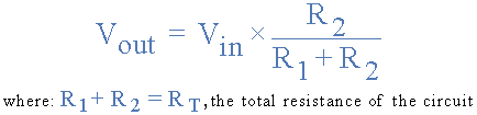
We also know that the capacitive reactance of a capacitor in an AC circuit is given as:
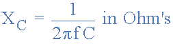
Opposition to current flow in an AC circuit is called impedance, symbol Z and for a series circuit consisting of a single resistor in series with a single capacitor, the circuit impedance is calculated as:
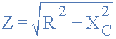
Then by substituting our equation for impedance above into the resistive potential divider equation gives us:
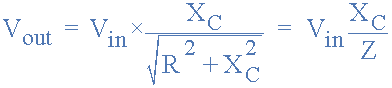
So, by using the potential divider equation of two resistors in series and substituting for impedance we can calculate the output voltage of an RC Filter for any given frequency.
Example No1
A Low Pass Filter
circuit consisting of a resistor of 4k7Ω in series with a capacitor of
47nF is connected across a 10v sinusoidal supply. Calculate the output voltage
(Vout) at a frequency of 100Hz and again at frequency of 10,000Hz or 10kHz.
At a frequency of 100Hz.
|
|
|
|
|
|
|
|
|
|
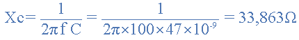
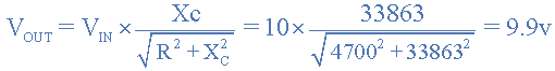
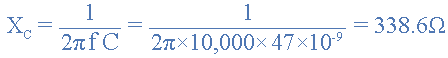
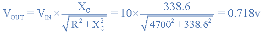
Frequency Response
We can see above, that as the frequency increases from 100Hz to 10kHz, the output voltage (Vout) decreases from 9.9v to 0.718v. By plotting the output voltage against the input frequency, the Frequency Response Curve or Bode Plot function of the low pass filter can be found, as shown below.
Figure 13.3
Frequency Response of a 1st-order Low Pass Filter
|
|
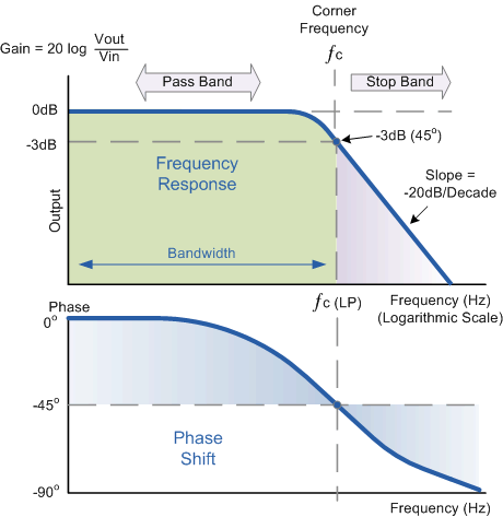
The Bode Plot shows the Frequency Response of the filter to be nearly flat for low frequencies and all of the input signal is passed directly to the output, resulting in a gain of nearly 1, called unity, until it reaches its Cut-off Frequency point ( ƒc ). This is because the reactance of the capacitor is high at low frequencies and blocks any current flow through the capacitor. After this cut-off frequency point the response of the circuit decreases giving a slope of -20dB/ Decade or (-6dB/Octave) "roll-off" as signals above this frequency become greatly attenuated, until at very high frequencies the reactance of the capacitor becomes so low that it gives the effect of a short circuit condition on the output terminals resulting in zero output.
For this type of Low Pass Filter circuit, all the frequencies below this cut-off, ƒc point that are unaltered with little or no attenuation and are said to be in the filters Pass band zone. This pass band zone also represents the Bandwidth of the filter. Any signal frequencies above this point cut-off point are generally said to be in the filters Stop band zone and they will be greatly attenuated.
This "Cut-off", "Corner" or "Breakpoint" frequency is defined as being the frequency point where the capacitive reactance and resistance are equal, R = Xc = 4k7Ω. When this occurs the output signal is attenuated to 70.7% of the input signal value or -3dB (20 log (Vout/Vin)) of the input. Although R = Xc, the output is not half of the input signal. This is because it is equal to the vector sum of the two and is therefore 0.707 of the input. As the filter contains a capacitor, the Phase Angle ( Φ ) of the output signal LAGS behind that of the input and at the -3dB cut-off frequency ( ƒc ) and is -45o out of phase. This is due to the time taken to charge the plates of the capacitor as the input voltage changes, resulting in the output voltage (the voltage across the capacitor) "lagging" behind that of the input signal. The higher the input frequency applied to the filter the more the capacitor lags and the circuit becomes more and more "out of phase".
The cut-off frequency point and phase shift angle can be found by using the following equation:
Cut-off
Frequency (Break Point Frequency) and Phase Shift
|
|
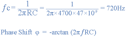
Then for our simple example of a "Low Pass Filter" circuit above, the cut-off frequency (ƒc) is given as 720Hz with an output voltage of 70.7% of the input voltage value and a phase shift angle of -45o.
Second-order Low Pass Filter
Thus far we have seen that simple first-order RC low pass filters can be made by connecting a single resistor in series with a single capacitor. This arrangement then gives us a -20dB/decade attenuation of frequencies above the cut-off point at ƒ3dB . However, sometimes this -20dB/decade (-6dB/octave) angle of the slope is not enough to remove an unwanted signal then two stages of filtering can be used instead
High Pass Filters
A High Pass Filter or HPF, is the exact opposite to that
of the previously seen Low Pass filter circuit, as now the two
components have been interchanged with the output signal (Vout) being taken
from across the resistor as shown.
Where the low pass filter only allowed signals to pass below its cut-off
frequency point, ƒc, the passive high pass filter circuit as its name implies,
only passes signals above the selected cut-off point, ƒc eliminating any low
frequency signals from the waveform. Consider the circuit below.
Figure 13.4 The High Pass Filter Circuit
|
|
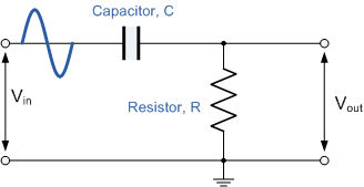
In this circuit arrangement, the reactance of the capacitor is very high
at low frequencies so the capacitor acts like an open circuit and blocks any
input signals at Vin until the cut-off frequency point (ƒc) is reached. Above
this cut-off frequency point the reactance of the capacitor has reduced
sufficiently as to now act more like a short circuit allowing all of the input
signal to pass directly to the output as shown below in the High Pass Frequency
Response Curve.
Figure 13.5 Frequency Response of a 1st Order High Pass Filter.
|
|
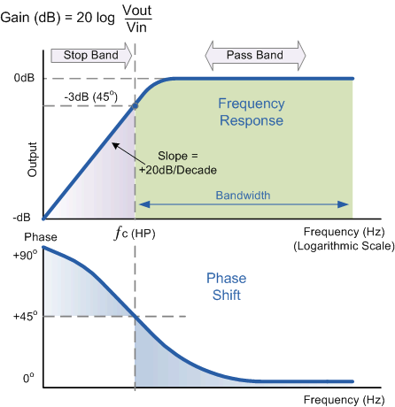
The Bode Plot or Frequency Response Curve above for a High Pass
filter is the exact opposite to that of a low pass filter. Here the signal is
attenuated or damped at low frequencies with the output increasing at +20dB/Decade
(6dB/Octave) until the frequency reaches the cut-off point (ƒc) where again R =
Xc. It has a response curve that extends down from infinity to the cut-off
frequency, where the output voltage amplitude is 1/√2 = 70.7% of the
input signal value or -3dB (20 log (Vout/Vin)) of the input value. The phase
angle ( Φ ) of the output signal LEADS that of the input and is
equal to +45o at frequency ƒc. The frequency response curve
for a high pass filter implies that the filter can pass all signals out to
infinity. However in practice, the high pass filter response does not extend to
infinity but is limited by the characteristics of the components used.
The cut-off frequency point for a first order high pass filter can be
found using the same equation as that of the low pass filter, but the equation
for the phase shift is modified slightly to account for the positive phase
angle as shown below.
Cut-off Frequency ( Break point) and Phase Shift
|
|
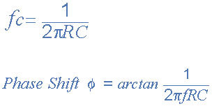
Notice the formula for
break-point frequency is of the same basic form as for the low-pass filter,
this helps keep things simple.
The circuit gain, Av which is given as Vout/Vin (magnitude) and is
calculated as:
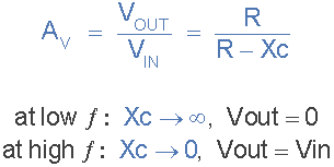
Example No1.
Calculate the cut-off or
"breakpoint" frequency (ƒc) for a simple high pass filter
consisting of an 82pF capacitor connected in series with a 240kΩ resistor.
|
|
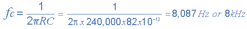
Active Filters
Above we saw how basic first-order filter circuits, such as the low pass and the high pass filters can be made using just a single resistor in series with a non-polarized capacitor connected across a sinusoidal input signal. We also noticed that the main disadvantage of passive filters is that the amplitude of the output signal is less than that of the input signal, i.e., the gain is never greater than 1 and that the load impedance affects the filter’s characteristics. With passive filter circuits containing multiple stages, this loss in signal amplitude called "Attenuation" can become quiet severe. One way of restoring or controlling this loss of signal is by using amplification through the use of Active Filters.
As their name implies, Active Filters contain active components such as operational amplifiers, transistors or FET's within their circuit design. They draw their power from an external power source and use it to boost or amplify the output signal. Filter amplification can also be used to either shape or alter the frequency response of the filter circuit by producing a more selective output response, making the output bandwidth of the filter narrower or even wider.
An active filter generally uses an operational amplifier (op-amp) within its design and earlier we saw that an Op-amp has a high input impedance, a low output impedance and a voltage gain determined by the resistor network within its feedback loop. Unlike a passive high pass filter which has in theory an infinite high frequency response, the maximum frequency response of an active filter is limited to the Gain/Bandwidth product (or open loop gain) of the operational amplifier being used. Still, active filters are generally easier to design than passive filters; they produce good performance characteristics, very good accuracy with a steep roll-off and low noise when used with a good circuit design.
Active Low Pass Filter
The most common and easily understood active filter is the Active Low Pass Filter. Its principle of operation and frequency response is exactly the same as those for the previously seen passive filter; the only difference this time is that it uses an op-amp for amplification and gain control. The simplest form of a low pass active filter is to connect an inverting or non-inverting amplifier.
First Order Active Low Pass Filter
|
|
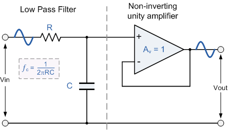
This first-order low pass active filter, consists simply of a passive RC filter stage providing a low frequency path to the input of a non-inverting operational amplifier. The amplifier is configured as a voltage-follower (Buffer) giving it a DC gain of one, Av = +1 or unity gain as opposed to the previous passive RC filter which has a DC gain of less than unity. The advantage of this configuration is that the op-amps high input impedance prevents excessive loading on the filters output while its low output impedance prevents the filters cut-off frequency point from being affected by changes in the impedance of the load.
While this configuration provides good stability to the filter, its main disadvantage is that it has no voltage gain above one. However, although the voltage gain is unity the power gain is very high as its output impedance is much lower than its input impedance. If a voltage gain greater than one is required we can use the following filter circuit.
Active Low Pass Filter with Amplification
|
|

The frequency response of the circuit will be the same as that for the passive
RC filter, except that the amplitude of the output is increased by the pass
band gain, AF of the amplifier. For a non-inverting amplifier
circuit, the magnitude of the voltage gain for the filter is given as a
function of the feedback resistor (R2) divided by its corresponding
input resistor (R1) value and is given as:
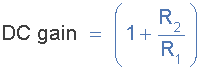
Therefore, the gain of an active low pass filter as a function of frequency will be:
Gain of a first-order low pass filter
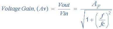
- Where:
- AF = the pass band gain of the filter, (1 + R2/R1)
- ƒ = the frequency of the input signal in Hertz, (Hz)
- ƒc = the cut-off frequency in Hertz, (Hz)
Thus, the operation of a low pass active filter can be verified from the frequency gain equation above as:
|
1. At very low frequencies, ƒ < ƒc, |
|
|
|
|
|
2. At the cut-off frequency, ƒ = ƒc, |
|
|
|
|
|
3. At very high frequencies, ƒ > ƒc, |
|
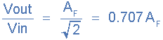
Thus, the Active Low Pass Filter has a constant gain AF from 0Hz to the high frequency cut-off point, ƒC. At ƒC the gain is 0.707AF, and after ƒC it decreases at a constant rate as the frequency increases. That is, when the frequency is increased tenfold (one decade), the voltage gain is divided by 10. In other words, the gain decreases 20dB (= 20log 10) each time the frequency is increased by 10. When dealing with filter circuits the magnitude of the pass band gain of the circuit is generally expressed in decibels or dB as a function of the voltage gain, and this is defined as:
Magnitude of Voltage Gain in (dB)
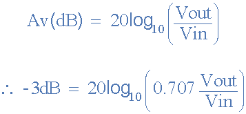
Example No1
Design a non-inverting active low pass filter circuit that has a gain of ten at low frequencies, a high frequency cut-off or corner frequency of 159Hz and an input impedance of 10KΩ.
|
The voltage gain of a non-inverting operational amplifier is given as: |
|
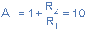
Assume a value for resistor R1 of 1kΩ rearranging the formula above gives a value for R2 of
|
|
then, for a voltage gain of 10, R1 = 1kΩ and R2 = 9kΩ. However, a 9kΩ resistor does not exist so the next preferred value of 9k1Ω is used instead.
converting this voltage gain to a decibel dB value gives:
|
|
The cut-off or corner frequency (ƒc) is given as being 159Hz with an input impedance of 10kΩ. This cut-off frequency can be found by using the formula:
|
|
where ƒc = 159Hz and R = 10kΩ. |
then, by rearranging the above formula we can find the value for capacitor C as:
|
|
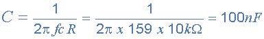
Then the final circuit along with its frequency response is given below as:
Low Pass Filter Circuit.
|
|
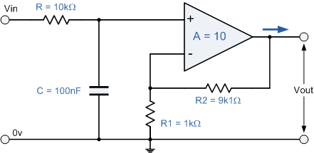
Frequency Response Curve
|
|
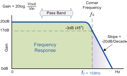
If the external impedance connected to the input of the circuit changes, this change will also affect the corner frequency of the filter (components connected in series or parallel). One way of avoiding this is to place the capacitor in parallel with the feedback resistor R2. The value of the capacitor will change slightly from being 100nF to 110nF to take account of the 9k1Ω resistor and the formula used to calculate the cut-off corner frequency is the same as that used for the RC passive low pass filter.
|
|
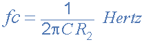
An example of the new Active Low Pass Filter circuit is given as.
Simplified non-inverting amplifier filter circuit
|
|
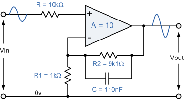
Equivalent inverting amplifier filter circuit
|
|
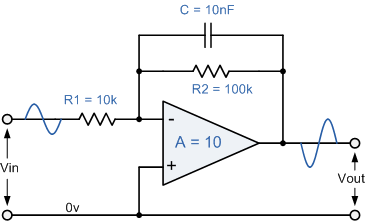
Applications of Active Low Pass Filters are in audio amplifiers, equalizers or speaker systems to direct the lower frequency bass signals to the larger bass speakers or to reduce any high frequency noise or "hiss" type distortion. When used like this in audio applications the active low pass filter is sometimes called a "Bass Boost" filter.
When cascading together filter circuits to form higher-order filters,
the overall gain of the filter is equal to the product of each stage. For
example, the gain of one stage may be 10 and the gain of the second stage may
be 32 and the gain of a third stage may be 100. Then the overall gain will be
32,000, (10 x 32 x 100) as shown below.
Cascading
Voltage Gain
|
|
|
|
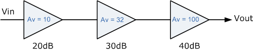
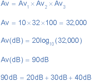
Active High Pass Filters
The basic operation of an Active High Pass Filter (HPF) is exactly the same as that for its equivalent RC passive high pass filter circuit, except this time the circuit has an operational amplifier or op-amp included within its filter design providing amplification and gain control. Like the previous active low pass filter circuit, the simplest form of an active high pass filter is to connect a standard inverting or non-inverting operational amplifier to the basic RC high pass passive filter circuit as shown.
First Order Active High Pass Filter
|
|
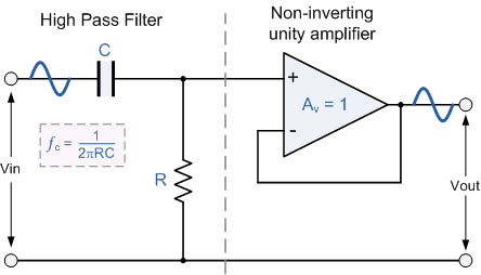
Technically, there is no such thing as an active high pass filter. Unlike Passive High Pass Filters which have an "infinite" frequency response, the maximum pass band frequency response of an active high pass filter is limited by the open-loop characteristics or bandwidth of the operational amplifier being used, making them appear as if they are band pass filters with a high frequency cut-off determined by the selection of op-amp and gain.
In the Operational Amplifier tutorial we saw that the maximum frequency response of an op-amp is limited to the Gain/Bandwidth product or open loop voltage gain ( A V ) of the operational amplifier being used giving it a bandwidth limitation, where the closed loop response of the op amp intersects the open loop response. A commonly available operational amplifier such as the uA741 has a typical "open-loop" (without any feedback) DC voltage gain of about 100dB maximum reducing at a roll off rate of -20dB/Decade (-6db/Octave) as the input frequency increases. The gain of the uA741 reduces until it reaches unity gain, (0dB) or its "transition frequency" ( Ft ) which is about 1MHz. This causes the op-amp to have a frequency response curve very similar to that of a first-order low pass filter and this is shown below.
Frequency response curve of a typical Operational Amplifier.
|
|
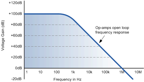
Then the performance of a "high pass filter" at high frequencies is limited by this unity gain crossover frequency which determines the overall bandwidth of the open-loop amplifier. The gain-bandwidth product of the op-amp starts from around 100kHz for small signal amplifiers up to about 1GHz for high-speed digital video amplifiers and op-amp based active filters can achieve very good accuracy and performance provided that low tolerance resistors and capacitors are used. Under normal circumstances the maximum pass band required for a closed loop active high pass or band pass filter is well below that of the maximum open-loop transition frequency. However, when designing active filter circuits it is important to choose the correct op-amp for the circuit as the loss of high frequency signals may result in signal distortion.
Active High Pass Filter
A first-order (single-pole) Active High Pass Filter as its name implies, attenuates low frequencies and passes high frequency signals. It consists simply of a passive filter section followed by a non-inverting operational amplifier. The frequency response of the circuit is the same as that of the passive filter, except that the amplitude of the signal is increased by the gain of the amplifier and for a non-inverting amplifier the value of the pass band voltage gain is given as 1 + R2/R1, the same as for the low pass filter circuit.
Active High Pass Filter with Amplification
|
|
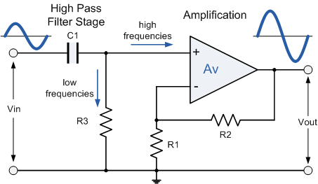
This first-order high pass filter, consists simply of a passive filter followed by a non-inverting amplifier. The frequency response of the circuit is the same as that of the passive filter, except that the amplitude of the signal is increased by the gain of the amplifier.
For a non-inverting amplifier circuit, the magnitude of the voltage gain for the filter is given as a function of the feedback resistor (R2) divided by its corresponding input resistor (R1) value and is given as:
Gain for an Active High Pass Filter
|
|
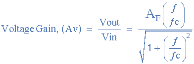
- Where:
- AF = the Pass band Gain of the filter, (1 + R2/R1)
- ƒ = the Frequency of the Input Signal in Hertz, (Hz)
- ƒc = the Cut-off Frequency in Hertz, (Hz)
Just like the low pass filter, the operation of a high pass active filter can be verified from the frequency gain equation above as:
|
1. At very low frequencies, ƒ < ƒc, |
|
|
|
|
|
2. At the cut-off frequency, ƒ = ƒc, |
|
|
|
|
|
3. At very high frequencies, ƒ > ƒc, |
|
Then, the Active High Pass Filter has a gain AF that increases from 0Hz to the low frequency cut-off point, ƒC at 20dB/decade as the frequency increases. At ƒC the gain is 0.707AF, and after ƒC all frequencies are pass band frequencies so the filter has a constant gain AF with the highest frequency being determined by the closed loop bandwidth of the op-amp. When dealing with filter circuits the magnitude of the pass band gain of the circuit is generally expressed in decibels or dB as a function of the voltage gain, and this is defined as:
Magnitude of Voltage Gain in (dB)
For a first-order filter the frequency response curve of the filter increases by 20dB/decade or 6dB/octave up to the determined cut-off frequency point which is always at -3dB below the maximum gain value. As with the previous filter circuits, the lower cut-off or corner frequency (ƒc) can be found by using the same formula:
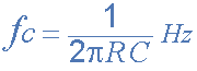
The corresponding phase angle or phase shift of the output signal is the same as that given for the passive RC filter and leads that of the input signal. It is equal to +45o at the cut-off frequency ƒc value and is given as:

A simple first-order active high pass filter can also be made using an inverting operational amplifier configuration as well, and an example of this circuit design is given along with its corresponding frequency response curve. A gain of 40dB has been assumed for the circuit.
Inverting Operational Amplifier Circuit
|
|
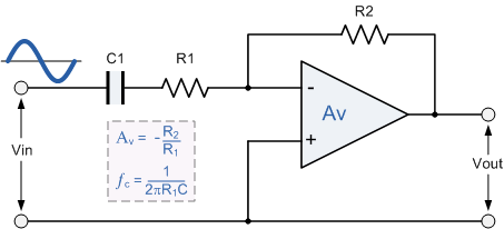
Frequency Response Curve
|
|
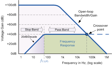
Example No1
A first order active high pass filter has a pass band gain of two and a cut-off corner frequency of 1kHz. If the input capacitor has a value of 10nF, calculate the value of the cut-off frequency determining resistor and the gain resistors in the feedback network. Also, plot the expected frequency response of the filter.
With a cut-off corner frequency given as 1kHz and a capacitor of 10nF, the value of R will therefore be:
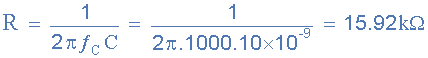
The pass band gain of the filter, AF is given as being, 2.
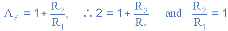
As the value of resistor, R2 divided by resistor, R1 gives a value of one. Then, resistor R1 must be equal to resistor R2, since the pass band gain, AF = 2. We can therefore select a suitable value for the two resistors of say, 10kΩ's each for both feedback resistors.
So for a high pass filter with a cut-off corner frequency of 1kHz, the values of R and C will be, 10kΩ's and 10nF respectively. The values of the two feedback resistors to produce a pass band gain of two are given as: R1 = R2 = 10kΩ's
The data for the frequency response bode plot can be obtained by substituting the values obtained above over a frequency range from 100Hz to 100kHz into the equation for voltage gain:
|
|
This then will give us the following table of data.
|
Frequency, ƒ |
Voltage Gain |
Gain, (dB) |
|
100 |
0.20 |
-14.02 |
|
200 |
0.39 |
-8.13 |
|
500 |
0.89 |
-0.97 |
|
800 |
1.25 |
1.93 |
|
1,000 |
1.41 |
3.01 |
|
3,000 |
1.90 |
5.56 |
|
5,000 |
1.96 |
5.85 |
|
10,000 |
1.99 |
5.98 |
|
50,000 |
2.00 |
6.02 |
|
100,000 |
2.00 |
6.02 |
The frequency response data from the table above can now be plotted as shown below. In the stop band (from 100Hz to 1kHz), the gain increases at a rate of 20dB/decade. However, in the pass band after the cut-off frequency, ƒC = 1kHz, the gain remains constant at 6.02dB. The upper-frequency limit of the pass band is determined by the open loop bandwidth of the operational amplifier used as we discussed earlier. Then the bode plot of the filter circuit will look like this.
The Frequency Response Bode-plot for our example.
|
|
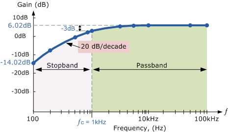
Applications of Active High Pass Filters are in audio amplifiers, equalizers or speaker systems to direct the high frequency signals to the smaller tweeter speakers or to reduce any low frequency noise or "rumble" type distortion. When used like this in audio applications the active high pass filter is sometimes called a "Treble Boost" filter.
Active Band Pass Filter
As we saw previously in the Passive Band Pass Filter tutorial, the principal characteristic of a Band Pass Filter or any filter for that matter, is its ability to pass frequencies relatively unattenuated over a specified band or spread of frequencies called the "Pass Band". For a low pass filter this pass band starts from 0Hz or DC and continues up to the specified cut-off frequency point at -3dB down from the maximum pass band gain. Equally, for a high pass filter the pass band starts from this -3dB cut-off frequency and continues up to infinity or the maximum open loop gain for an active filter.
However, the Active Band Pass Filter is slightly different in that it is a frequency selective filter circuit used in electronic systems to separate a signal at one particular frequency, or a range of signals that lie within a certain "band" of frequencies from signals at all other frequencies. This band or range of frequencies is set between two cut-off or corner frequency points labelled the "lower frequency" (ƒL) and the "higher frequency" (ƒH) while attenuating any signals outside of these two points.
Simple Active Band Pass Filter can be easily made by cascading together a single Low Pass Filter with a single High Pass Filter as shown.
|
|
The cut-off or corner frequency of the low pass filter (LPF) is higher than the cut-off frequency of the high pass filter (HPF) and the difference between the frequencies at the -3dB point will determine the "bandwidth" of the band pass filter while attenuating any signals outside of these points. One way of making a very simple Active Band Pass Filter is to connect the basic passive high and low pass filters we look at previously to an amplifying op-amp circuit as shown.
Active Band Pass Filter
|
|
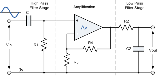
This cascading together of the individual low and high pass passive filters produces a low "Q-factor" type filter circuit which has a wide pass band. The first stage of the filter will be the high pass stage that uses the capacitor to block any DC biasing from the source. This design has the advantage of producing a relatively flat asymmetrical pass band frequency response with one half representing the low pass response and the other half representing high pass response as shown.
|
|
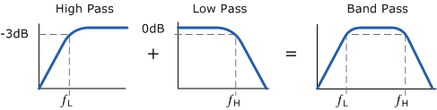
The higher corner point (ƒH) as well as the lower corner frequency cut-off point (ƒL) are calculated the same as before in the standard first-order low and high pass filter circuits. Obviously, a reasonable separation is required between the two cut-off points to prevent any interaction between the low pass and high pass stages. The amplifier provides isolation between the two stages and defines the overall voltage gain of the circuit. The bandwidth of the filter is therefore the difference between these upper and lower -3dB points. For example, if the -3dB cut-off points are at 200Hz and 600Hz then the bandwidth of the filter would be given as: Bandwidth (BW) = 600 - 200 = 400Hz. The normalised frequency response and phase shift for an active band pass filter will be as follows.
Active Band Pass Frequency Response
|
|
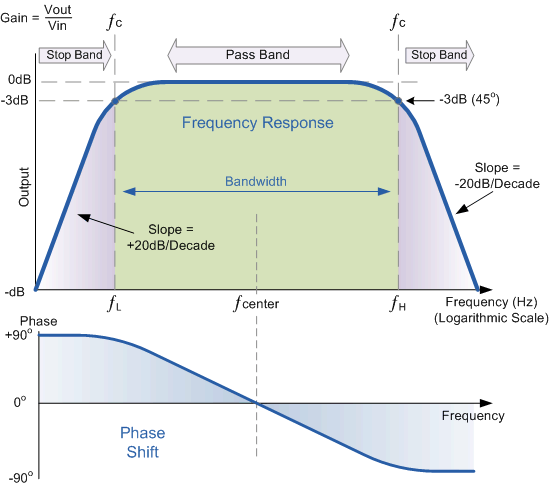
While the above passive tuned filter circuit will work as a band pass filter,
the pass band (bandwidth) can be quite wide and this may be a problem if we
want to isolate a small band of frequencies. Active band pass filter can also
be made using inverting operational amplifiers, and by rearranging the
positions of the resistors and capacitors within the circuit we can produce a
much better filter circuit as shown below. The lower cut-off -3dB point is
given by ƒC2 while the upper cut-off -3dB point is given by ƒC1.
Inverting Band Pass Filter Circuit
|
|
|
|
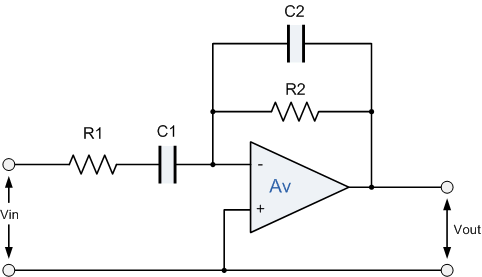
This type of band pass filter is designed to have a much narrower pass band.
The centre frequency and bandwidth of the filter is related to the values of
R1, R2, C1 and C2. The output of the filter is again taken from the output of
the op-amp.
Multiple Feedback Band Pass Active Filter
We can improve the band pass response of the above circuit by rearranging the components again to produce an infinite-gain multiple-feedback (IGMF) band pass filter. This type of active band pass design produces a "tuned" circuit based around a negative feedback active filter giving it a high "Q-factor" (up to 25) amplitude response and steep roll-off on either side of its centre frequency. Because the frequency response of the circuit is similar to a resonance circuit, this centre frequency is referred to as the resonant frequency, (ƒr). Consider the circuit below.
Infinite Gain Multiple Feedback Active Filter
|
|
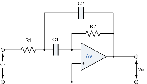
This active band pass filter circuit uses the full gain of the operational
amplifier, with multiple negative feedback applied via resistor, R2
and capacitor C2. Then we can define the characteristics of the IGMF
filter as follows:
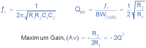
We can see then that the relationship between resistors, R1 and R2
determines the band pass "Q-factor" and the frequency at which the
maximum amplitude occurs, the gain of the circuit will be equal to -2Q2.
Then as the gain increases so to does the selectivity. In other words, high
gain - high selectivity.
Example No1
An active band pass filter that has a gain Av of one and a resonant frequency, ƒr of 1kHz is constructed using an infinite gain multiple feedback filter circuit. Calculate the values of the components required to implement the circuit.
Firstly, we can determine the values of the two resistors, R1 and R2 required for the active filter using the gain of the circuit to find Q as follows.
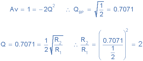
Then we can see that a value of Q = 0.7071 gives a relationship of resistor, R2 being twice the value of resistor R1. Then we can choose any suitable value of resistances to give the required ratio of two. Then resistor R1 = 10kΩ and R2 = 20kΩ.
The centre or resonant frequency is given as 1kHz. Using the new resistor values obtained, we can determine the value of the capacitors required assuming that C = C1 = C2.
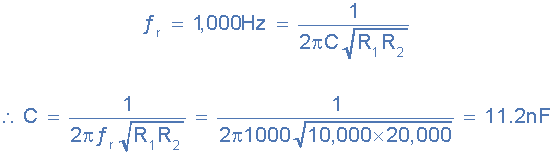
The closest standard value is 10nF.
Resonant Frequency
The actual shape of the frequency response curve for any passive or active band pass filter will depend upon the characteristics of the filter circuit with the curve above being defined as an "ideal" band pass response. An active band pass filter is a 2nd Order type filter because it has "two" reactive components (two capacitors) within its circuit design and will have a peak response or Resonant Frequency (ƒr) at its "centre frequency", ƒc. The centre frequency is generally calculated as being the geometric mean of the two -3dB frequencies between the upper and the lower cut-off points with the resonant frequency (point of oscillation) being given as:
|
|
- Where:
- ƒr is the resonant or Centre Frequency
- ƒL is the lower -3dB cut-off frequency point
- ƒH is the upper -3db cut-off frequency point
and in our simple example above the resonant centre frequency of the active band pass filter is given as:
|
|
The "Q" or Quality Factor
In a Band Pass Filter circuit, the overall width of the actual pass band between the upper and lower -3dB corner points of the filter determines the Quality Factor or Q-point of the circuit. This Q Factor is a measure of how "Selective" or "Un-selective" the band pass filter is towards a given spread of frequencies. The lower the value of the Q factor the wider is the bandwidth of the filter and consequently the higher the Q factor the narrower and more "selective" is the filter.
The Quality Factor, Q of the filter is sometimes given the Greek symbol of Alpha, (α) and is known as the alpha-peak frequency where:
|
|

As the quality factor of an active band pass filter (Second-order System) relates to the "sharpness" of the filters response around its centre resonant frequency (ƒr) it can also be thought of as the Damping Factor or Damping Coefficient because the more damping the filter has the flatter is its response and likewise, the less damping the filter has the sharper is its response. The damping ratio is given the Greek symbol of Xi, (ξ) where:
|
|
The "Q" of a band pass filter is the ratio of the Resonant Frequency, (ƒr) to the Bandwidth, (BW) between the upper and lower -3dB frequencies and is given as:
|
|
|
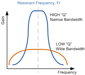
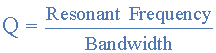
Then for our simple example above the quality factor "Q" of the band pass filter is given as:
346Hz / 400Hz = 0.865. Note that Q is a ratio and has no units.
When analysing active filters, generally a normalised circuit is considered which produces an "ideal" frequency response having a rectangular shape, and a transition between the pass band and the stop band that has an abrupt or very steep roll-off slope. However, these ideal responses are not possible in the real world so we use approximations to give us the best frequency response possible for the type of filter we are trying to design. Probably the best known filter approximation for doing this is the Butterworth or maximally-flat response. In the next tutorial we will look at higher order filters and use Butterworth approximations to produce filters that have a frequency response which is as flat as mathematically possible in the pass band and a smooth transition or roll-off rate.