


ESSENTIAL ELECTRONICS FOR A2 LEVEL by Dr Chris Barnes PhD Eng. QTS, MCIEA, GW4BZD.
PART 1 CONTROL AND MICROPROCESSOR BASED SYSTEMS
Chapter 1 Open- and closed-loop control
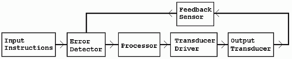
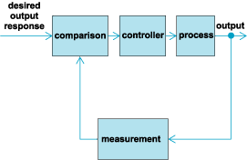
The basis for analysis of a control system is the foundation provided by linear system theory, which assumes a cause-effect relationship for the components of a system. A component or process to be controlled can be represented by a block. Each block possesses an input (cause) and output (effect). The input-output relation represents the cause-and-effect relationship of the process, which in turn represents a processing of the input signal to provide an output signal variable, often with power amplification. An open-loop control system utilizes a controller or control actuator in order to obtain the desired response (Fig. 1).
![]()
Open-loop
control system.
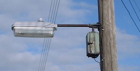
A good example would be a street light controller.
When the light level falls, the light sensor converting the light level to an electrical signal detects this. The comparator gives an output when its threshold level is crossed, and the driver then switches the lamp on. Good automatic streetlight systems will have the light sensor placed so that it cannot pick up the light from the lamp otherwise this would have affected the operation of the system. On the picture below you can see the sensor on top of the lampshade so that it can respond to the skylight and not to the lamp.
In contrast to an open-loop control system, a closed-loop control system utilizes an additional measure of the actual output in order to compare the actual output with the desired output response (Fig. 2). A standard definition of a feedback control system is a control system which tends to maintain a prescribed relationship of one system variable to another by comparing functions of these variables and using the difference as a means of control. In the case of the driver steering an automobile, the driver uses his or her sight to visually measure and compare the actual location of the car with the desired location. The driver then serves as the controller, turning the steering wheel. The process represents the dynamics of the steering mechanism and the automobile response.
Closed-loop
control system.
A feedback control system often uses a function of a prescribed relationship between the output and reference input to control the process. Often, the difference between the output of the process under control and the reference input is amplified and used to control the process so that the difference is continually reduced. The feedback concept has been the foundation for control system analysis and design.
Applications for feedback systems
Familiar control systems have the basic closed-loop configuration. For example, a refrigerator has a temperature setting for desired temperature, a thermostat to measure the actual temperature and the error, and a compressor motor for power amplification. Other examples in the home are the oven, furnace, and water heater. In industry, there are controls for speed, process temperature and pressure, position, thickness, composition, and quality, among many others. In the automotive industry feedback control is used for ABS and for Cruise Control. In electronic communications closed loop control is used to achieve ALC in transmitters, AGC in receivers and even in automatic matching in ATUS (Automatic antenna tuning units). Feedback control concepts have also been applied to mass transportation, electric power systems, automatic warehousing and inventory control, automatic control of agricultural systems, biomedical experimentation and biological control systems, and social, economic, and political systems.
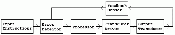
A practical closed loop control system
Control systems have input sensors which generate signals that instruct the system to act. The instructions specify what the control system should do. It could be something simple like a voltage used to specify how bright a lamp should be. It could be more complex like a binary code used to change a TV channel. Here are some examples...
Resistive Transducers:
Switches:
Start, Stop, Reset, Sense machinery position.
Combination Lock.
Pressure mat.
Resistors
LDR for light level measurement.
Thermistor for temperature measurement.
Potentiometer for angle measurement.
Potentiometer for setting a reference voltage.
Strain gauge.
Sound sensors:
Microphone, Ultrasound sensor.
Time information:
Astable produces timed pulses which trigger the control system to act.
A microcontroller that has computer code to instruct the control system to act.
Digital logic circuit
Logic gates, Counters, Shift registers, Latches.
Microcontroller
Analogue input.
Digital inputs and outputs.
Analogue circuits
Comparator.
Schmitt trigger.
Summing Amplifier.
Difference Amplifier.
These are needed to drive the output transducers. Mostly the processor has insufficient power to drive these output devices. If higher power circuits like railway locomotives need to be controlled, complex high power driver circuits are needed. Most output devices need some sort of driver.
MOSFET Switch
MOSFET Source Follower
BJT Switch
BJT Emitter Follower
Voltage Follower
Relay
H Bridge Driver
It could be anything from a single light bulb to the avionic controls for an entire aircraft.
Motors
Conventional
Stepper
Servo
Light
Bulbs
LEDs
LASERs
LED Displays
Seven Segment
LED matrix
LCD Displays
Sound
Piezoelectric Sounder
Loud Speaker
Buzzer
Siren
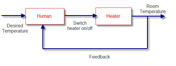
Closed loop control applied to heating simplest possible case
feedback path for heat
Real central heating system
When the home is cold, the heat sensor detects this and turns on the heater via a comparator giving an output to the driver at the switch-on temperature. The heater then produces heat, which eventually warms up the home. This is the feedback signal, for the heat sensor detects this warmth and eventually will turn off the heater. This system is also known as an on-off or bang-bang control system. The heater can only be switched fully on even if the home is just below the required temperature.
The automatic streetlight characteristics are illustrated by this graph of its input/output behaviour:
Light level
threshold
level
Lamp 12 noon 12midnight 12 noon
on
off
When the light level drops below the threshold level, the lamp switches on.
The home heater characteristics are illustrated by this graph:
Home temp.
threshold
level
Heater
on
off
The heater output affects the home temperature and this will result in the heater switching on and off repeatedly.
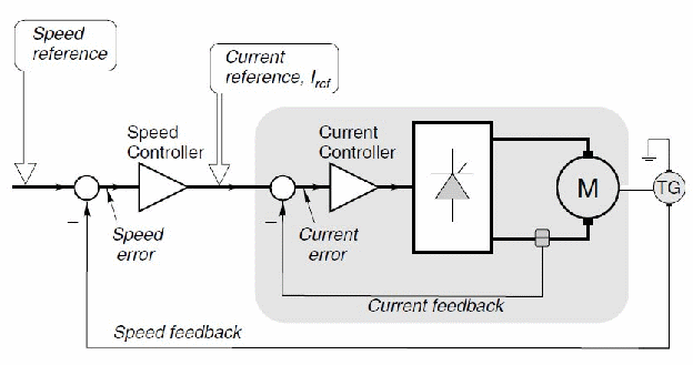
Simple motor speed (Servo control)

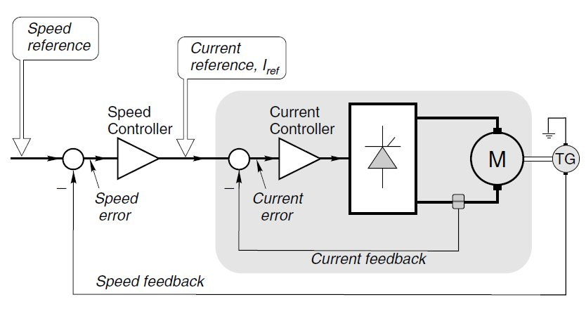
More sophisticated motor control with both current and speed feedback
In the following questions use these codes for your answers:
input = A feedback = B negative = C
output = D positive = E process = F
Which of the above:
Takes a signal from the environment?
Is missing from an open-loop control system?
Has some action on the input signal in a control system?
Produces a signal detectable in the environment?
Is used only in a closed-loop control system?
When used in a system gives control over the desired output? (2
codes required, enter 2nd code in answer to question 7.)
Enter here the 2nd part of answer to question 6
Drives the output of a system to an extreme when used
as a feedback signal?
Results in the output switching on and off continually, maintaining
a desired output level? (2 codes required, enter 2nd code in
answer to question 10.)
Enter here the 2nd part of your answer to question 9.
Digital computer systems
The use of a digital computer as a compensator device has grown since 1970 as the price and reliability of digital computers have improved.
Within a computer control system, the digital computer receives and operates on signals in digital (numerical) form, as contrasted to continuous signals. The measurement data are converted from analog form to digital form by means of a converter. After the digital computer has processed the inputs, it provides and output in digital form, which is then converted to analog form by a digital-to-analog converter. See also Analog-to-digital converter; Digital-to-analog converter.
Automatic handling equipment for home, school, and industry is particularly useful for hazardous, repetitious, dull, or simple tasks. Machines that automatically load and unload, cut, weld, or cast are used by industry in order to obtain accuracy, safety, economy, and productivity. Robots are programmable computers integrated with machines. They often substitute for human labor in specific repeated tasks. Some devices even have anthropomorphic mechanisms, including what might be recognized as mechanical arms, wrists, and hands. Robots may be used extensively in space exploration and assembly. They can be flexible, accurate aids on assembly lines. See also Robotics.
Microprocessor Systems and Sub Systems
Binary data features in these systems as with logic and counter
A BIT, is a BINARY DIGIT.
A bit can be a zero or a 1.
A binary number made of eight bits, such as 11001010 is known as a BYTE.
Four bits, such as 1101 is known as a NIBBLE (half a byte and a joke).
Sixteen bits numbers are a WORD.
Thirty two bits ones are a LONG WORD.
Sixty four bits numbers are a VERY LONG WORD.
These numbers can be stored in REGISTERS inside chips (integrated circuits).
1k in binary systems is 1024.
These collections of bits can represent binary numbers. They can also represent decimal or other number systems.
The ASCII system uses them to represent the letters of the alphabet and punctuation. The ASCII TABLE gives the binary equivalents of the alphabet.
All this information is called DATA.
Numbers in microprocessor systems are often expressed in hexadecimal.
Indeed, most numbers and values for microprocessors are written as hexadecimal numbers. These can be written in several ways, including: - FA16, FAh, &HFA, 0xFA, 0XFA
The microprocessor is also called the CENTRAL PROCESSING UNIT (CPU).
There are very many cpu's and one of the most common is the 6502.
Buses
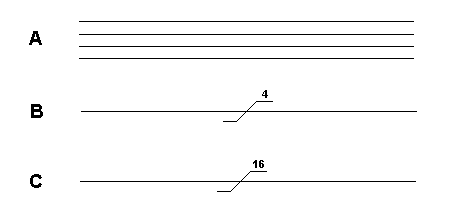
A bus is a collection of wires. Diagram A is a four bit bus. Zeros and ones can be put on the bus, 0 volts for zero and +5 volts to represent a one. The smallest number that can be put on a four bit bus is 0000. The largest is 1111 which is 15 in decimal and F in hex. Therefore sixteen different numbers can be placed on this bus, 0000 being the lowest and 1111 the highest. Rather than draw four wires, we use the representation shown in diagram B.
Many microprocessor systems use a eight bit data bus. The smallest number that can be placed on it is 00000000. The largest number is 11111111 which is equivalent to 255 in decimal. Therefore 256 different numbers can be placed on this bus. 255 in decimal is FF in hex.
A sixteen bit bus is shown in diagram C. The smallest number we can put on this bus is 0000000000000000. The largest number is 1111111111111111 which is 65535 in decimal. Therefore 65536 different numbers can be put on this bus. 65535 in decimal is FFFF in hex.
All the registers in the memory chips have their own individual addresses, like house numbers in a street. By putting its address, in binary, on an address bus we can select any individual register. Address buses are commonly 16 bits, so we can select any one of 65536 registers.
Microprocessor System Diagram Architecture of Generalised Microprocessor System.
There are two main types of architecture found in microprocessor control systems. The traditional von Neumann architecture uses a single set of wires (bus) along which both program and data instructions are fetched. This is the architecture on which most multi IC microprocessor control systems are based. The other common system is known as the Harvard architecture and in this the program instructions and the data are accessed on separate buses. This architecture is usually used in single IC microcontroller systems, e.g. PICs and AVRs and enables a much greater processing rate to be achieved.
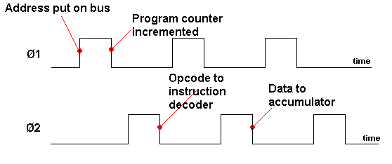
A generalized von Neumann type programmable system is shown below showing the main sections. Each of the sections is connected to three sets of wires known as 'buses'.
The CPU can put a binary number on the address bus, to select an individual register in the ROM or ram or the I/O. The arrows on this bus show that addresses go one way only. Data at the selected address can be put on the data bus.
The CPU can also put data on this bus which can be written into a register of ram or i/o. It is not possible to write data into ROM (read only memory). This is shown by the single arrow on the ROM data bus and double arrows on the other two. The control bus instructs the chips to do various things, such as when to read or write etc.
The clock tells all the chips when to change what they are doing. Like the drill sergeant who shouts "LEFT, RIGHT, LEFT, RIGHT". The crystal control the speed of operation. In simple systems Memory chips are simply a collection of registers, each with its own address. Data, in the form of 0's and 1's, is stored in the registers.
ROM
ROM chips can be read from, but not written to. They are non volatile, which means that they retain their contents after power is removed. Most ROMs are programmed during manufacture of the chips.
Others, PROGRAMMABLE ROMS, PROMS, can have their contents programmed in after manufacture. The 2716 ROM shown above is an EPROM.
This is an erasable prom, where if you make a mistake, you can erase the contents by shining ultra-violet light through a window in the chip.
Some chips are ELECTRICALLY ERASABLE and are known as EEPROMS..
PIC CHIPS and AVRS have their own built in ROM
RAM
RAM means random access memory. A better name would be read/write memory. Ram is VOLATILE, meaning that when you switch off, the data it contains is lost.
There are two main types of ram, static and dynamic.
Static ram uses flip-flops to store bits, and so consumes current whether they are storing a 1 or a 0. Dynamic ram uses capacitors to store charges and use less power.
However, these stored charges leak away and have to be continually REFRESHED which makes the circuitry more complicated.
As an example, the 4118 is an 8 bit x1k static ram having an 8 bit data bus, D0-D7.
Data can be written to, or read from memory, depending the state of the WE pin. There may be several memory chips, so only one is selected at a time by taking the CS pin low.
Just as with ROM, micro-controllers such as PIC CHIPS and AVRS have their own built in ROM and so can be regarded as tiny computers on a single chip.
The Clock
Keeps the whole system synchronized
The clock is usually a square wave generator whose frequency is controlled by a crystal. In a typical control system it oscillates at between 1-8 MHz (1-8 million times a second) and controls the speed at which the system operates. But in computer systems it may be thousands of times faster than this rate.
Tristate Logic
As we saw earlier, Buses are the transport system for the electronic signals that pass between the sections of the control system. There are three main types of signals that are needed:-
a) data
b) addresses
c) control signals.
The data and address signals are multi-bit digital signals sent in parallel, usually with +5V representing a logic 1 and 0V representing logic 0, although there are some systems available with logic 1 being represented by voltages as low as 1.1V.
The control signals are often one bit digital signals.
Buses are used to prevent a proliferation of connections between the various sections of a programmable control system. Usually there is a separate bus for each of the three types of signals although there are some systems that use a shared bus for the data and address signals.
A bus can be thought of as being like a railway line connecting several stations together. Trains travel between the stations using the same track. Obviously, with a railway, care must be taken to ensure that two different trains do not require the track at the same time. The same is also true for electronic signals.
The data bus carries information around the system and is bi-directional. It is connected to all sections of the system.
These various sections need to be able to put information onto and take information from the data bus and so need to be physically connected to it. Reading information from the data bus is not a problem since all of the various sections of the system have high impedance inputs.
Putting information (writing) onto the data bus is more of a problem, since only one device can write data at a time. If two (or more) devices were to try to put data onto the data bus at the same time there would be a bus contention. This would be like two trains using the same section of track at the same time! Smoke would come out of somewhere! The short circuit would either cause one of the devices to fail or the track connecting them to melt.
To overcome this problem, all devices which put data onto the data bus are connected through Tri-state drivers. These drivers have three possible states -
"high", "low" and "disconnected", i.e. +5V, 0V and floating
This is so that when the device is NOT selected, its output just floats up and down with the signals on the data bus and so do not interfere with the data bus signals.
The
tri-state drivers are controlled by the address bus and control lines
and have an
output enable, (OE) control pin which
makes their outputs high impedance when the (OE) pin is logic
1. Many devices for use on data buses have tri-state drivers built
into them,
e.g. analogue to digital converters, (ADCs), memory
devices etc.
Every device in the microprocessor system that needs to receive or send data, outside the processor, needs a unique address. The address bus is used to carry the address signals around the system, and each device is connected either directly to the address bus or to an address decoder that is connected to the address bus.
The number of unique addresses is directly determined by the width of the address bus (number of separate wires). A 16 bit address bus can address 216, or 65536 different memory locations while a 32 bit address bus has 232, i.e. 4,294,967,296 addresses, a maximum of 4 gigabytes of directly addressable memory.
The control bus consists of signals from the processor and is mostly one bit. The actual number of control signals depends upon the type of processor used but some typical control signals are discussed below.
The read/write (R/W) control signal. When the microprocessor wants to read information from memory or from an input port it signals this by setting the R/W line to logic 1. When the microprocessor wants to write information into memory or to an output port it signals this by setting the R/W line to logic 0.
The Chip Select (CS) control signal. This is used when the microprocessor wants to access a peripheral chip
Interrupt requests
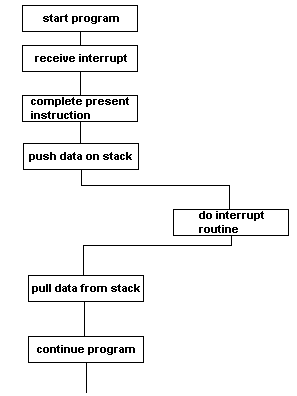
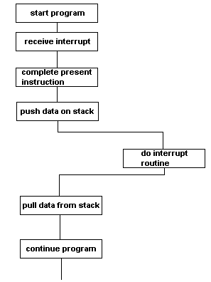
The microprocessor system may be measuring temperatures in the Sahara desert. Once a year it receives a radio signal telling it to stop measuring temperatures and send all last year's data to base. This is an INTERRUPT.
The CPU completes its current instruction. It then pushes any data it wishes to save onto the stack. It then jumps to a routine which services the interrupt. Once the interrupt routine is completed, it pulls the saved data from the stack and carries on measuring temperatures. There are two pins on the CPU which, when taken low, cause hardware interrupts.
IRQ can be sensed or ignored whichever depends on the value of the interrupt flag in the status register.
As we have seen most of the time the flow of data in or out of the processor through the data bus is controlled by the program code operating in the processor. But there are events that occur in a processor control system that must not wait. These include inputs from the keyboard, co-processors and messages from input/output ports to indicate that processes are complete (such as conversions by A to D converters.) or that the mains power has failed. The attention of the processor is attracted when the IRQ line is taken to logic 0. The processor will then finish executing the current instruction, save all of the current values in its registers, identify which device has requested an interrupt and then service the interrupting device. When this is completed the processor will return to the task it was doing before the interrupt occurred. Interrupts via the IRQ line are known as Maskable Interrupts because they can be disabled by the programmer, for time-sensitive routines.
There is
another interrupt request line which cannot be disabled.
This is
known as the Non-maskable Interrupt (NMI) line. When
taken to logic 0 it has the same effect as the IRQ line. The
use of the NMI line is usually restricted to very important
devices i.e. hard disk drives, etc.
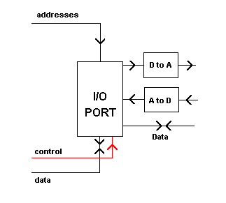
Inputs and Outputs
Input and output devices are connected to microprocessor systems through ports.
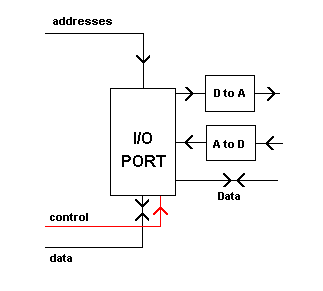
A microprocessor system is pointless unless it can communicate with the outside world. It does this through an INTERFACE which is usually a plug or socket.
The CPU communicates with this interface via an INPUT/OUTPUT PORT chip.
These chips are called VERSATILE INTERFACE ADAPTORS or UNIVERSAL ASYNCHRONOUS RECEIVER/TRANSMITTERS (UARTS) etc.
Ports have their own registers with addresses, and the CPU can write data to, or read data from, these registers. If the system is controlling a set of traffic lights, then the CPU can write data to the registers, to switch the lights in the correct sequence. It can also read data that is provided to the port by sensors buried in the road.
This means that it can make decisions according to the amount of traffic and switch the lights accordingly. Since the system is digital and the outside world is mostly analogue, digital to analogue converters are required when providing an output, such as one to control the temperature of an oven.
An analogue to digital converter is required if the system is to read an analogue device, such as a thermometer.
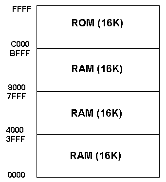
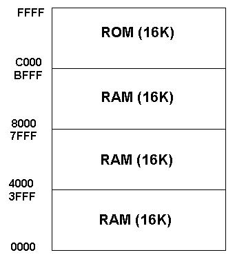
The memory map shows how addresses have been allocated for memory and any other devices connected to the address bus. Here ram has been given the lowest 48k of addresses and ROM the highest 16k. Each area of memory can be subdivides into pages of 256 addresses.
Page zero occupies addresses 0000 to 255 in decimal or 0000 to 00FF in hex.
Page zero occupies addresses 0000 to 255 in decimal or 0000 to 00FF in hex
Some microprocessors require these ports to be addressed as part of the overall memory and are said to be Memory Mapped. The most efficient way of making inputs and outputs is through memory mapping where I/O ports are made to look like memory addresses. Address decoders accompany this method.
Other microprocessors use a separate control signal, Memory/Input-Output (M/IO), to switch between memory addresses and input/output addresses.
These ports are said to be I/O Mapped.
Some microprocessors require these ports to be addressed as part of the overall memory and are said to be Memory Mapped.
There are advantages and disadvantages to each system. In general, both systems use the Address Bus to provide the address of the port. Memory mapping of I/O ports is easy to implement and the resulting ports are treated and programmed just like any other memory location. However, it does restrict the amount of RAM and ROM that can be connected to the microprocessor. The diagram opposite shows a circuit to decode a 16 bit memory address to a memory mapped port at the address 00FF16. The output will be a logic 1 when the memory address is 00FF16 and the address is selected, i.e. CS is logic 0.
I/O mapping of ports requires the microprocessor to have the additional M/IO control line. The status of this line determines whether the information on the address bus is a memory address or the address of an I/O port. As a result, this additional control signal has to be included into the address decoding for every memory location, so making I/O mapping more complex to implement. However, I/O mapping does have the advantage that it does not restrict the amount of RAM and ROM that can be addressed by the microprocessor.
Microprocessors
that have a M/IO
control line usually only use the first 8 bits of their address bus
for addressing I/O ports. The diagram opposite shows the equivalent
I/O mapped circuit to decode an I/O mapped port at the address FF16.
The output will be a logic 1 when the memory address
is FF16, the address is selected, ie CS
is logic 0 and M/IO
is
logic 0.
While this is a simpler circuit than the equivalent Memory Mapped circuit, it should be remembered that the M/IO control line has to be incorporated every time there is information on the address bus, i.e. for every memory location.
There are many other control lines that are used by microprocessors. The Intel Pentium D processor, for example, has in excess of 100 separate control lines. It also has 64 data bus lines, 36 memory address lines, 226 positive power supply connections and 273, 0V connections!
PIC and AVR Microcontrollers
Associated with all programmable systems from PICS to PCs, the latter of which are really only complex programmable systems has grown a set of words and phrases or jargon. The more common ones are listed below along with their meanings.
|
bit |
binary digit, is a single 1 or 0 from a binary number |
|
byte |
8 bits, usually used to represent one character |
|
address |
A number which refers to each unique memory element in RAM and ROM. |
|
data |
the information read by and written from the processor. |
|
read |
when the processor takes in information or data from either ROM, RAM or the input port. |
|
write |
when the processor gives out information or data to either the RAM or the output port. |
|
hardware |
the general name for the actual electronic circuits that make up the programmable system. |
|
software |
the general name for the instructions that are followed by the processor. |
|
bus |
a common set of wires connecting together the memory elements of a programmable system. There are two main buses:- |
|
data bus |
responsible for carrying all of the information |
|
address bus |
carries the information to identify which memory element is required |
|
tristate buffer |
a
device to which the output of each memory element is connected. |
|
registers |
data is stored here before or after processing. The number and type of registers depends on the processor. |
|
accumulator(s) |
these are special registers into which the result of any arithmetic or logical process is placed. Some processors have more than one accumulator. In microcontrollers the accumulator is usually known as the Working Register |
|
flag register |
A special register where each of eight bits (Flags) indicate certain features of the last computation made. These flags can be used to determine what happens next. e.g. |
|
a zero flag |
is set to 1 if the result of the last operation was zero; |
|
a sign flag |
is set to 1 to indicate if the content of the Accumulator is negative; |
|
a carry flag |
that indicates if the maximum number has been exceeded. |
|
arithmetic
logic unit |
performs arithmetic or Boolean logic operations on the data. |
|
program counter (PC) |
This contains the address of the next instruction. |
|
instruction decoder |
This interprets each program instruction into a set of electronic conditions that make the data move around appropriately through the processor, and operates the control lines. |
|
stack pointer (SP) |
is a register containing the address of a region of memory called; |
|
the stack |
The stack is used as a temporary store for data, and grows in size as data is added, falling as data is removed. It is often located at the top of the memory with the current stack value decreasing as the stack fills up It is used sequentially i.e. last in, first out. The stack pointer is needed to identify the end of the stack. |
|
|
|
The concept of having a complete microcontroller (processor, RAM and ROM) on a single chip was far sighted in that such devices would enable the simplification of much of the circuitry required for electronic control of commercial, industrial and domestic equipment. Two companies in America began work on such SoCs in the late 1980s. Microchip Technologies produced the PIC (Programmable Interface Controller) in the early 1990s and Atmel released the AVR soon after. The success of these devices is largely due to their cost and processing ability. Since they are programmable devices they can be used in many applications and so can be mass produced which ensures low cost. Both PICs and AVRs are based on the Harvard architecture and initially incorporate 8-bit Reduced Instruction Set Computer (RISC) processor having only a few tens of instructions. This small number of instructions also improved the take up and use of these devices as they did not require the high degree of training needed to program them when compared to processors having Complex Instruction Sets Computer (CISC).
Since there are separate buses for the program instructions and data information, the instructions do not have to be restricted to being 8-bits wide like the data. In fact the early PICs used a 12-bit instruction set, later moving to 16-bits for some of the more complex devices. The AVRs use as standard a 16-bit word format for their instructions. The use of separate data and program buses enables 'pipe-lining' to be implemented so that while one instruction is being executed, the next instruction is pre-fetched from the program memory. This enables instructions to be executed in every clock cycle.
The early success of these devices prompted the manufacturers to add more facilities onto the chip including real time clocks, counter / timers, power on reset circuitry, Input and Output ports, Analogue to Digital Converters, Serial Input and Output ports etc. The whole chip is implemented in Complementary Metal Oxide Semiconductor (CMOS) and so has an inherent low power consumption. This coupled with a sleep mode makes them suitable for battery operated equipment as well. The clock speed of PICs and AVRs is wide ranging and many will operate at clock frequencies as high as 80MHz. While this may seem slow compared to the latest Intel processors, the specially optimised instruction set and with programs written in machine code, instructions ensures that they are able to carry out many operations and processes very quickly and efficiently.
In order to show the differences between the architecture of PICs/AVRs and discrete IC programmable controllers, a generic block diagram is shown below. It is based on one common family of PIC devices, the PIC16CXX. The major difference between the block diagram of a PIC and AVR device is that the instruction address bus and program data buses are 16-bit wide instead of the 12-bits shown in the diagram.
The actual number of ports on the devices depends upon the type number but it is not unusual for there to be as many as four parallel ports, a serial port, and four analogue to digital converter ports on some of the more complex PICs and AVRs.
Generic block diagram of a PIC/AVR.
Social
and Economic Implications of Single IC
Programmable Control
Systems (SoCs)
The effect of single IC programmable control systems on modern life has been significant. They have permeated all areas of modern appliances and machines and their effect will continue to increase as more powerful devices are developed. They are already used extensively in modern domestic appliances, e.g. washing machines, microwave cookers, video recorders, CD players etc. with the result that complex features can be incorporated into them as standard features. Most modern road vehicles have Engine Management Systems (EMS) controlling the operation of the engine. The heart of the EMS is a PIC or AVR which not only is able to maintain the efficient operation of the engine but is also able to monitor the operation of the engine and determine when servicing is required as well as help diagnose faults. Vehicles are just beginning to appear which have many programmable controllers incorporated which are able to monitor every aspect of the car, not just the engine. As a result, if it rains the windscreen wipers are switched on; if it goes dark the lights are turned on etc. without the driver having to take any action. Such cars obviously have ABS as a standard fitting which is controlled by a programmable controller. With so many electronic systems on board, the repair and maintenance of such vehicles becomes a specialised business.
The availability of many cheap computer peripherals e.g., printers, digital cameras, scanners etc. is also largely due to the use of control SoCs. They are able to monitor precisely the mechanical operation of these items and correct for imperfections in the mechanics of the peripheral. The result is that less precise mechanisms can be used, so reducing cost, but the controller is able to maintain the overall quality.
Each mobile phone has its own programmable control system on board to take care of the frequency management as the phone moves from one cell to another. Since this is a vital role but one that does not use a significant amount of processing power, it leaves the processor free for other tasks, like managing an address/phone number data base, generating ever complex (and annoying) ring tones, running games on the phone screen etc. However, since a mobile phone has to communicate with the local base station regularly when it is switched on so that the mobile phone system knows that it is available to receive calls, it means that the location of the phone is also known to within a few hundred metres. So you cannot hide if you have a mobile phone switched on!
The next major development with SoCs will be in their use in Smart cards. These will be the next version of credit and bank cards which will be able to store information about the owner as well as be used for intelligent information exchange in shops etc. The potential growth in this market is very large.
With the increasing complexity of the software used in microcontroller systems, it becomes very difficult to ensure that the software is reliable under all of the operating conditions that may be encountered. While it may be an inconvenience if a fault in the software causes the front door on a microprocessor controlled washing machine to suddenly open while the machine is full of water, software faults in engine management systems could be fatal. Consider the theoretical situation in which a car, with a microcontroller engine management system, pulls out to overtake a vehicle. The driver sees an oncoming vehicle in the distance and in order to ensure a completely safe overtake, changes into a lower gear. However, if an undetected software fault in the EMS causes the engine to falter and a crash results, no evidence of the software fault would be found in the subsequent enquiry, and the driver would be blamed for the accident.
There is still controversy surrounding the crash of the Mk2 Chinook helicopter ZD576 on the Mull of Kintyre in 1994, in which 29 people died including the two pilots, Flight lieutenants Trapper and Cook. In the subsequent Ministry of Defence enquiry, the pilots were found guilty of gross negligence. However, subsequent enquiries and press interest (mainly Computer Weekly) have raised questions about the reliability of the software used in the engine control system on the aircraft.
It is therefore vital that all software is fully and exhaustively tested to ensure that all operating conditions are covered reliably.
In the first 7 questions use these codes for your answers:
address bus = 1 clock = 4 processor = 7
control bus = 2 input port = 5 RAM = 8
data bus = 3 output port = 6 ROM = 9
Which one of the above:
Carries data within the control system?
Keeps the whole control system synchronised?
Provides permanent storage of data?
Is connected to the outside world? (2 codes, lowest first)
Carries information to select the required memory element?
Performs logic or arithmetic operations?
Provides temporary storage of data?
Give a disadvantage of using a microcontroller over an
electromechanical system?
A = cost B = repairability C = flexibility D = long life
State the number of chips used in PIC system.
How many output states has a tri-state logic gate?
Programming
The AQA GCE Specification states that candidates should be able to:
analyze a process into a sequence of fundamental operations;
convert a sequence of fundamental operations into a flow chart;
interpret flow charts and convert them into a generic microcontroller program;
recognize and use a limited range of assembler language microcontroller instructions (see Data Sheet, Appendix E);
write
subroutines to:
configure the input and output pins
read
data from a sensor
write data to an output device
give a
specified time delay
give a specified sequence of control
signals
perform simple arithmetic and logic operations
detect
events using polling and hardware interrupts;
compare the use of
hardware interrupts and polling to trigger events;
interpret
programs written with a limited range of assembler instructions.
It is not therefore the intention of this section of this book to attempt to make every student into an expert programmer, there are other complete GCE A levels and even Degree Courses for this.
An appendix, however, on understanding and programming a specific PIC chip has been included for completeness.
Here the aim is for students to gain sufficient knowledge of programming to be able to test any electronic systems including PICS that they might design. Although with some exam boards specific use of PICS in prcatical work is not a pre-requisite.
In the commercial world, once the electronics engineer has developed and perfected the electronic system, it would then be handed over to a programmer to write the control program that will be used in the actual product.
However, whether writing test programs or the fully functional program for the system, it is essential that the ability to think logically is developed and that complex sequences of operations can be broken down into small, simple sequences that can then be translated into programs.
Flow chart diagrams are one of several graphical methods that can be used to aid logical thought and are employed to help determine the sequence of operations required
Flow charts are easy-to-understand diagrams showing how steps in a process fit together. This makes them useful tools for communicating how processes work, and for clearly documenting how a particular job is done. Furthermore, the act of mapping a process out in flow chart format helps you clarify your understanding of the process, and helps you think about where the process can be improved. In this respect they are often used by Systems Analysts when thinking how to computerize a process such as issuing and return of library books or DVD videos in a shop.
A flow chart can therefore be used to:
Define and analyze processes.
Build a step-by-step picture of the process for analysis, discussion, or communication.
Define, standardize or find areas for improvement in a process
Also, by conveying the information or processes in a step-by-step flow, you can then concentrate more intently on each individual step, without feeling overwhelmed by the bigger picture.
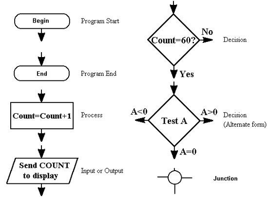
Three main types of symbol:
Elongated circles, which signify the start or end of a process.
![]()
Rectangles, which show instructions or actions.
![]()
Diamonds, which show decisions that must be made
Within each symbol, write down what the symbol represents. This could be the start or finish of the process, the action to be taken, or the decision to be made.
Symbols are connected one to the other by arrows, showing the flow of the process.
To draw the flow chart, brainstorm process tasks, and list them in the order they occur. Ask questions such as "What really happens next in the process?" and "Does a decision need to be made before the next step?" or "What approvals are required before moving on to the next task?"
Start the flow chart by drawing the elongated circle shape, and labeling it "Start".
Then move to the first action or question, and draw a rectangle or diamond appropriately. Write the action or question down, and draw an arrow from the start symbol to this shape.
Work through your whole process, showing actions and decisions appropriately in the order they occur, and linking these together using arrows to show the flow of the process. Where a decision needs to be made, draw arrows leaving the decision diamond for each possible outcome, and label them with the outcome. And remember to show the end of the process using an elongated circle labeled "Finish".
Finally, challenge your flow chart. Work from step to step asking yourself if you have correctly represented the sequence of actions and decisions involved in the process. And then (if you're looking to improve the process) look at the steps identified and think about whether work is duplicated, whether other steps should be involved, and whether the right people are doing the right jobs.
Tip:
Flow charts can quickly
become so complicated that you can't show them on one piece of paper.
This is where you can use "connectors" (shown as numbered
circles) where the flow moves off one page, and where it moves onto
another. By using the same number for the off-page connector and the
on-page connector, you show that the flow is moving from one page to
the next.
Flow charts are simple diagrams that map out a process so that it can easily be communicated to other people.
To draw a flowchart, brainstorm the tasks and decisions made during a process, and write them down in order.
Then map these out in flow chart format using appropriate symbols for the start and end of a process, for actions to be taken and for decisions to be made.
Finally, challenge your flow chart to make sure that it's an accurate representation of the process, and that that it represents the most efficient way of doing the job.
When planning software, one of the stages is to produce a flow chart. The shape of the box indicates its function. Further data is given as text inside the box.
Example Flow Charts
This system is of an electronically controlled fan that will monitor the air temperature every 60 seconds and decide whether the fan should be on or off.
START
delay 60s
input
temperature
is
temperature
over 20oC?
fan on fan off
Since this system would run indefinitely, there is no END terminal box. The use of the loop means that the operations are described once, but every 60 seconds the flowchart is used again and again. The label in each input/output box tells you which type it is.
The flow diagram is self explanatory and shows the correct use of the various symbols.
It is good practice to try to analyse everyday basic tasks into the separate steps that could be put into a flow chart and then to try writing a flow chart for that task, e.g. design a flow chart to produce a soft-boiled egg.
It is useful to remember that most programmable systems are very simple and can only operate on one instruction at a time. There should be no multiple processes going on at the same time in any flow chart!
When designing flow charts, it is useful to identify each of the operations needed for a particular process. The following examples may help.
Consider a
programmable control system reading in data from a sensor. If the
sensor is analogue then it will need an
Analogue to Digital
Converter (ADC) to change the analogue signal into a digital signal
which the control system can understand.
A detailed description of
ADCs is given in the next chapter on Input Subsystems, but for the
moment it is sufficient to know that an ADC needs a short logic 0
signal to be applied to its
Start Conversion (SC) pin in order to
make the conversion process start. When the ADC has finished the
conversion,
it sets its End of Conversion (EoC) pin to logic 1.
A
suitable flow chart for this process is shown opposite.
In this flow chart the processor keeps checking to see when the EoC pin of the ADC becomes logic 1. Such an operation is known as 'polling' and while it is very simple to implement it does use the full processing power of the processor and so stops the processor from carrying out any other operations. In the vast majority of cases this is not a problem and so is often used in simple test programs.
While some
programmable systems have real time clocks that can be used for time
delays, many do not. An easy way of generating a delay is to make
the processor execute a simple program a large number of times. Such
time delay loops are not accurate enough for time keeping because of
any interrupt routines that may run during the timing operation, but
are suitable when the time period is not critical.
The flow chart
for a simple time delay is shown opposite.
Writing data to an output port can be a simple process unless there is a large amount of data to transfer to a slow output device.
Consider an example where the output device is slow.
If there was no flow control for the data between the process controller and the output device then the output device would not be able to keep up with the transfer of data and so information would be lost.
To prevent this, a flow control system has to be established. This often takes the form of the process controller sending a pulse to the output device when there is valid data for the output device to read.
The output
device will then set a 'Wait' control line, say to
logic 1, as an
indication to the process controller that it should wait and not send
any more data.
When the output device has 'digested' the data it then sets the Wait control line to logic 0.
The process controller detects this and so makes the next byte of data available.
A flow diagram to enable this process to occur is shown opposite. It is worth noting the point in the program at which the process controller sends the signal to say that the data is available.
Converting Flowcharts into Programs
In order to be able to fully test a programmable system, it is obviously necessary to be able to write sufficient programs to activate every section. In order to do this it is essential for the electronics engineer to have some programming skills. The same skills for programming are required no matter what programming language is being used, the most important skills being to think logically, be able to break complex operations into single step functions and to remember that the programmable system will only do what you tell it to, which is not necessarily the same as what you want it to do!
There are three main types of programming languages:-
Machine code, the 1s and 0s that the machine understands directly,
Interpreted languages, including some Assemblers, Basic, Pascal, Visual Basic etc.
Compiled languages including some Assemblers, Delphi, C++ etc.
Despite the general move to Object Orientated Languages, there is little new in programming. Modern computers work so much faster and have much more storage capacity than they did in the past that modern languages take advantage of this. No matter what processor is being used, it will only be able to understand instructions that are written in its native language, Machine Code. These instructions consist of numbers and for most people are completely incomprehensible. Associated with each machine code instruction is a mnemonic, a sort of English abbreviation to explain what the instruction does.
The following examples are machine code instructions for the Intel 80X86 series of processors:-
the instruction 0x93, has a mnemonic XCHG BX, AX and means exchange the contents of the BX and AX registers whilethe instruction 0xBA1C0F, which has a mnemonic of MOV DX, 0F1C and means move or load the number 0F1C into register DX.
Assembly language is a language that will translate the mnemonics into machine code. This can be done in one of two ways depending upon the Assembly language. Some interpret the instructions when the program is executed, i.e. they will take each mnemonic instruction, translate it into machine code and then execute the machine code instruction.
Other Assembly language programs, when executed, will translate each mnemonic instruction into a machine code instruction and then store these machine code instructions in a separate place in memory, i.e. it Compiles the machine code instructions. Once all of the mnemonic instructions have been compiled the processor will then execute the machine code instructions.
As can be seen from the above descriptions Interpreted programs run slower than Compiled programs, but with modern processors operating so fast, and Interpreted programs being more interactive, they are eminently suitable for the testing of programmable systems.
While Assembler makes some attempt to use recognisable words as instructions, higher level languages e.g. Basic, Pascal, C, Java, Python etc. use English phrases as the instructions. These are then Interpreted or Compiled to machine code instructions for execution.
Sub routines
It makes sense when writing programs to break them up into small sections that can easily be tested (just like the actual electronic systems themselves which are built and tested as subsystems). These small sections have various names depending upon which program is used. ‘Basic’ calls them Subroutines, while Pascal calls them Procedures and C++ calls them Objects. These small sections can then be accessed from the main program when needed.
For example, a subroutine could be written to send data to an output port. Then whenever data has to be sent to this port, the data is passed to the subroutine, which outputs the data and then returns control back to the main program.
The AQA Microcontroller and Assembly Language.
The AQA specification assumes a generic microcontroller with a Harvard architecture and the following specification:-
a clock speed of between 1 and 20MHz;
an accumulator or working register, W, through which all calculations are performed;
a program counter, PC;
three 8-bit bi-directional ports - PORTA, PORTB and PORTC;
Three
data direction registers TRISA, TRISB and TRISC,
to determine whether the bits of each port are inputs or outputs.
If a bit is set to 1 then the port bit is an input, if the bit is
set to 0 then the port bit is an output.
E.g. if TRISA =
0x01, then bit D0 of PORTA is an input and bits D1
to D7 of PORTA are outputs.
a status register, SR, for which bit 0 is the carry flag, C, and bit 2 is the zero flag, Z;
A
clock prescaler, PRE, which can be set to divide the clock
frequency by 2 to 256.
If PRE is set to 1, then the clock
frequency is divided by 2. If PRE is set to 2 then the clock
frequency is divided by 3, etc
In general, the clock frequency is
divided by PRE + 1.
If PRE is set to 0, then the
timing function is disabled;
an 8-bit timer register, TMR, which is decremented on each falling edge of the clock prescaler pulse and which sets bit 1 of the status register, SR, when it is 0.
This specification requires candidates to be familiar with a limited range of assembler language microcontroller instructions which are listed on the next page and will also be available on the Data sheet included with the examination paper.
Within the Assembler Language Instructions it is useful to note:-
the memory is made up of registers, each with its own separate address, R;
the
contents of a register are indicated by putting the register address
in brackets
e.g. (R)
K is
used to represent a literal,
which can be a memory
location (e.g. 0x29),
a label (e.g. display) or
a value, (e.g.
0xFA);
standard arithmetic and Boolean operators, e.g. add K to W etc;
the number of clock cycles needed to execute an instruction, since this will affect the response time of the system;
the Flags that are affected by each of the instructions;
Comments
can be added to instructions by writing them after either a
semicolon; or a double forward slash //. E.g.
NOP ; This
instruction takes one clock cycle to execute
NOP // This
instruction takes one clock cycle to execute.
After a Master Reset (or when the power is switched on), the program counter register PC is set to zero (0x00) which makes the microcontroller start to execute the instructions at address 0x00. The microcontroller will continue to execute the instructions in order unless the value in PC is changed either by a Jump instruction or a subroutine Call instruction.
|
Mnemonic |
Operands |
Description |
Operation |
Flags |
Clock cycles |
|
NOP |
none |
No operation |
none |
none |
1 |
|
CALL |
K |
Call Subroutine |
stack <=PC PC <= K |
none |
2 |
|
RET |
none |
Return from Subroutine |
PC <= stack |
none |
2 |
|
|
|
|
|
|
|
|
INC |
R |
Increments the contents of R |
(R) <= (R) + 1 |
Z |
1 |
|
DEC |
R |
Decrements the contents of R |
(R) <= (R) - 1 |
Z |
1 |
|
|
|
|
|
|
|
|
ADDW |
K |
Add K to W |
W <= W + K |
Z, C |
1 |
|
ANDW |
K |
AND K with W |
W <= W • K |
Z, C |
1 |
|
SUBW |
K |
Subtract K from W |
W <= W - K |
Z, C |
1 |
|
ORW |
K |
OR K and W |
W <= W + K |
Z, C |
1 |
|
XORW |
K |
XOR K and W |
W <= W Å K |
Z, C |
1 |
|
|
|
|
|
|
|
|
JMP |
K |
Jump to K (GOTO) |
PC <= K |
none |
2 |
|
JPZ |
K |
Jump to K on zero |
PC <= K if Z=1 |
Z=1 |
2 |
|
JPC |
K |
Jump to K on carry |
PC <= K if C=1 |
C=1 |
2 |
|
|
|
|
|
|
|
|
MOVWR |
R |
Move W to the contents of R |
(R) <= W |
Z |
1 |
|
MOVW |
K |
Move K to W |
W <= K |
Z |
1 |
|
MOVRW |
R |
Move the contents of R to W |
W <= (R) |
Z |
1 |
|
|
|
|
|
|
|
Assembly Language Instructions
|
NOP |
This instruction has no effect on any of the registers or flags. But it does take one clock cycle to execute and so can be used to create short time delays and can be useful for synchronising input and output operations.
|
|
CALL K |
Subroutines are a useful way of being able to make frequently needed groups of instructions available anywhere within a program. They are also a convenient way of breaking up a program into manageable sections. To transfer execution to a subroutine, the instruction CALL is used. CALL is followed by the memory address of the start of the subroutine or the label pointing to the start of the subroutine, e.g. CALL 0x7B, CALL delay The CALL instruction takes 2 clock cycles to execute because it has to store the current value of the program counter, PC, onto the stack, decrement value in the stack pointer, and then load the address of the subroutine into the program counter. Call does not alter any Flags.
|
|
RET |
This instruction is used to end a subroutine and transfer execution back to the main program. It does not take any additional information and does not alter any flags. It does take 2 clock cycles to execute and this should be considered in systems where there are time constraints. In operation, the last value stored in the stack is loaded into the PC and the value in the stack pointer is incremented.
|
|
INC R DEC R |
These instructions are used to increase or decrease the contents of a register by 1. Both instructions take one clock cycle and so are quickly executed. Both instructions are followed by the register address. In operation, the contents of the register is increased or decreased by 1 and the result stored back in the register. If, as a result of these instructions, 0 is loaded back into the register, then the Zero flag, Z, is set.
|
|
ADDW K ANDW K SUBW K ORW K XORW K |
These instructions provide arithmetic and Boolean operations. All take one clock cycle to execute. They operate on the contents of the Working register, W, and restore the resulting value back in W. If the value loaded back into W is zero then the Z flag is set to 1. If the value loaded back into W is greater than 255 or less than 0, then the Carry flag, C, is set to 1.
|
|
JMP K |
This instruction is used to change the location of the next instruction to be executed. It differs from the CALL instruction as no return address is stored. It can be thought of as a GOTO instruction. The JMP instruction is followed by the address of the next instruction to be executed or a label pointing to the address, e.g. JMP 0x7B or JMP delay In operation, this address is loaded into the program counter, PC and takes 2 clock cycles to execute.
|
|
JPZ K |
This instruction is used to change the location of the next instruction to be executed ONLY IF the zero flag, Z, is set. It is followed by the address of the next instruction to be executed or a label pointing to the address, e.g. JPZ 0x7B or JPZ delay In operation, if Z is 1, then this address is loaded into the program counter, PC. If Z is 0 then the PC is not changed. Either way the instruction takes 2 clock cycles to execute.
|
|
JPC K |
This instruction is used to change the location of the next instruction to be executed ONLY IF the carry flag, C, is set. It is followed by the address of the next instruction to be executed or a label pointing to the address, e.g. JPC 0x7B or JPC delay In operation, if C is 1, then this address is loaded into the program counter, PC. If C is 0 then the PC is not changed. Either way the instruction takes 2 clock cycles to execute.
|
|
MOVWR R |
This instruction is used to move the contents of the W register into the register R. It takes 1 clock cycle to execute and the zero flag, Z, is set if the value stored in R is 0.
|
|
MOVW K |
This instruction is used to move the value, K, into the working register, W. It takes 1 clock cycle to execute and the zero flag, Z, is set if the value stored in W is 0.
|
|
MOVRW R |
This instruction is used to move the contents of the register, R, into the working register W. It takes 1 clock cycle to execute and the zero flag, Z, is set if the value stored in W is 0.
|
Using Assembly Language Instructions
Below are some examples of the use of assembly language instructions for some frequently used operations. It is assumed in all of these examples that the microcontroller has a clock speed of 1MHz.
Setting the direction of the bits of a port.
The system needs PORTA to have D0, D1, D2 to be inputs and D3 to D7 to be outputs.
This is achieved by:-
working out the binary value to be written to the data direction register TRISA,
converting it to hexadecimal,
moving this value into the working register, W,
moving the contents of W into TRISA.
Since a 1 sets the bit to input and a 0 sets the bit to output, the binary value is 00000111.
This is 0x07 as a hexadecimal number.
To put this value into W, the instruction is MOVW 0x07.
To move W to TRISA, the instruction is MOVWR TRISA.
So the assembler code is
MOVW 0x07
MOVWR TRISA
This technique can be applied to any of the bits of any of the ports of the microcontroller and takes 2µs to execute.
Masking bits in registers.
There are many occasions where it is just the value of a particular bit within a register that is of interest e.g. an input bit of a port, a flag within the status register, SR, etc. masking is achieved by ANDing the value in the register with a value that reduces all unwanted bits to 0.
Consider the following example.
PORTA has been set so that D0, D1, D2 are inputs and the other bits are outputs.
The system needs to know the value of just D0 and D1.
To mask all of the other bits it is necessary to work out the binary value when D0 and D1 are both 1 and all of the other bits are 0. This gives a value of 00000011 = 0x03.
If the
value of PORTA is moved to W and then ANDed with 0x03,
all of the bits except
D0 and D1 will be
turned to zero.
To move PORTA into W, the instruction is MOVRW PORTA
To AND W with 0x03, the instruction is ANDW 0x03
So the assembler code is
MOVRW PORTA
ANDW 0x03
Generating a very short time delay
This is usually achieved by repeatedly using the NOP instruction. Each NOP instruction takes 1µs to execute and so
NOP
NOP
NOP
NOP
NOP
generates a time delay of 5µs
Generating a time delay
It is wasteful of memory to produce time delays longer than a few microseconds using the technique above. The microcontroller has special facilities to achieve longer time delays which are based on two special registers, the prescaler register, PRE, and the timer register, TMR. They can be thought of as being arranged as below.
PRE is used to divide the clock frequency by a ratio that can be programmed into it. If PRE has the value of 1, then the clock frequency is divided by 2, if PRE has a value of 2, then the clock frequency is divided by 3, etc. In general the clock frequency is divided by PRE + 1.
The maximum value that the clock frequency can be divided by is 256.
If PRE is set to 0, then the timing functions are disabled.
The operation of PRE and TMR is independent of what ever else the microcontroller is doing, so the microcontroller can be carrying out other tasks while awaiting for the delay to occur.
The value in the TMR register decreases by 1 on each falling edge of the pulses from PRE. To obtain a particular time delay, the values to load into PRE and TMR need to be carefully chosen. Often there is more than one set of values that will achieve the delay.
E.g. A delay of 2ms is needed, and the microcontroller has a clock frequency of 1MHz.
One way of achieving this delay is to load PRE with 7 (0x07), which will then divide the clock frequency by 8, so giving a period of 8µs. If TMR is then loaded with 250 (0xFA), it will decrease by one every 8µs and so will reach 0 after 2ms and then set bit 1 of the status register, SR.
The same
result could also be achieved by loading PRE with 124 (0x7C)
and TMR
with 16 (0x10).
The following assembler instructions are used to load PRE and TMR with the first set of values:-
MOVW 0x07 // Move 7 (0x07) into W
MOVWR PRE // Move the contents of W into PRE
MOVW 0xFA // Move 250 (0xFA) into W
MOVWR TMR // Move the contents of W into TMR
To detect when TMR reaches zero, bit 1 of SR can be polled by the microcontroller.
This can be achieved by:-
moving SR into W,
ANDing W with 0x02 to mask all but bit 1
Jumping back to the start if the zero flag is set.
When the time period has finished, bit 1 will be 1 and so the jump will not occur.
So the full assembly instructions to achieve a 2ms delay are:-
MOVW 0x07 // Move 7 (0x07) into W
MOVWR PRE // Move the contents of W into PRE
MOVW 0xFA // Move 250 (0xFA) into W
MOVWR TMR // Move the contents of W into TMR
loop1: // Label for the start of the checking loop
MOVRW SR // Move the contents of SR into W
ANDW 0x02 // AND the contents of W with 2
JPZ loop1 // Jump to loop1 if the zero flag is not set, i.e. TMR is not zero
It should be noted that the time delay from this program will be slightly longer than 2ms.
It takes 4µs to initially set up the PRE and TMR registers and there is an error of between 4 and 7µs from the last three lines of code depending on when exactly TMR becomes zero. For accurate timing these errors need to be considered and it would be more accurate to set TMR to 249 instead of 250 which would then give an error of between 0 and 3µs.
Generating a long time delay
The maximum delay that can be achieved with a 1MHz clock and PRE and TMR both set with 255 is approximately 65.5ms.
To achieve longer delays still it is necessary to use additional registers as counters.
The example below uses the 2ms delay code above to give a delay of 0.5s (500ms). A register with an address which will not interfere with either the stack or the program is chosen as an additional timing register. In this example the register at 0xA0 will be used.
To achieve a 500ms delay requires 250 loops of the 2ms delay, so the register 0xA0 is preloaded with 250 (0xFA) which is decreased by one on each loop until it reaches zero.
The assembly instructions for a 500ms delay are:-
// Set the value for PRE. Since this is not changed by the
// program it only needs to be set once.
MOVW 0x07 // Move 7 (0x07) into W
MOVWR PRE // Move the contents of W into PRE
// Set the value for the timing register 0xA0
MOVW 0xFA // Move 250 (0xFA) into W
MOVWR 0xA0 // Move the contents of W into 0xA0
// The 2ms delay
loop2: // Label for the 2ms delay
MOVW 0xF9 // Move 249 (0xF9) into W (corrected for timing errors)
MOVWR TMR // Move the contents of W into TMR
loop1: // Label for the start of the checking loop
MOVRW SR // Move the contents of SR into W
ANDW 0x02 // AND the contents of W with 2
JPZ loop1 // Jump to loop1 if the zero flag is not set, i.e. TMR is not zero
// Every 2ms the timing register value is decreased by 1
DEC 0xA0 // Decrement the value in register 0xA0
// Check if the value is zero.
JPZ end // Jump to end if the zero flag is set
JMP loop2 // Jump to loop2 if the zero flag is not set, i.e. (0xA0) is not zero
end: // label for the end of the timing loops
Again there will be timing errors which can be minimised by adjusting the value in TMR.
Even longer time delays can be obtained by having multiple additional timing registers cascaded together.
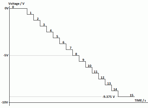
Digital Ramp ADC
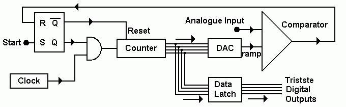
The output of a binary counter is connected to a DAC.
This produces a ramp wave.
A comparator is used to compare the ramp with the signal to be converted.
When the comparator changes state, the binary data is latched.
In this way the analogue input is converted to binary numbers.
The diagram below shows a 4 bit ADC. 8, 12 and 16 bit converters are
more common.
|
8 |
4 |
2 |
1 |
|
|
0 |
0 |
0 |
0 |
0 |
|
0 |
0 |
0 |
1 |
1 |
|
0 |
0 |
1 |
0 |
2 |
|
0 |
0 |
1 |
1 |
3 |
|
0 |
1 |
0 |
0 |
4 |
|
0 |
1 |
0 |
1 |
5 |
|
0 |
1 |
1 |
0 |
6 |
|
0 |
1 |
1 |
1 |
7 |
|
1 |
0 |
0 |
0 |
8 |
|
1 |
0 |
0 |
1 |
9 |
|
1 |
0 |
1 |
0 |
10 |
|
1 |
0 |
1 |
1 |
11 |
|
1 |
1 |
0 |
0 |
12 |
|
1 |
1 |
0 |
1 |
13 |
|
1 |
1 |
1 |
0 |
14 |
|
1 |
1 |
1 |
1 |
15 |
The ramp is this way up because the summing amplifier used in the DAC is also an inverting amplifier.
This type of ADC is fairly slow (but cheap and simple).
It is ideal for data that changes fairly slowly such as vehicle or aircraft control systems.
Audio signals are also slow enough to be converted.
To convert video, a flash ADC is needed.
The diagram below shows how an 8-bit ADC could be constructed with a microcontroller.
It also shows a
typical analogue input interface, which limits the input voltage
range to
-0.6V to 12V.
PORTA of the microcontroller supplies the DAC with the 8-bit digital input. Bit D0 of PORTB detects when the output of the comparator changes. When the output voltage from the DAC exceeds the analogue input voltage, the comparator output goes high. The 10kΩ resistor and 1N4148 diode protect the base of the transistor by limiting the base current and also stops the input becoming negative. With the output of the comparator high, the D0 input to PORTB will be logic 0.
The conversion is started by making SC logic 0.
A possible control program for the microcontroller is shown below:
// Set all bits of PORTA to be outputs
MOVW 0x00 // Move 0 into W
MOVWR TRISA // Move the contents of W to TRISA
// Set PORTB so that D0 and D1 are inputs
MOVW 0x03 // Move 3 into W
MOVWR TRISB // Move the contents of W to TRISB
// Check to see if SC is logic 0
start: // Label for loop to check if SC is logic 0
MOVRW PORTB // Move the contents of PORTB to W
// Mask all but bit D1
ANDW 0x02 // AND W with 2
JPZ main // Go to the main program if SC is logic 0
JMP start // Repeat the loop to check if SC is logic 0
main: // Label for the beginning of the main conversion program
// Set the input of the DAC to 0 by setting PORTA to 0
MOVW 0x00 // Move 0 to W
MOVWR PORTA // Move the contents of W to PORTA
loop1: //
Label for the beginning of the loop to check if the
//
conversion is complete
// Check to see if D0 is logic 0, i.e. conversion complete
MOVRW PORTB // Move the contents of PORTB to W
// Mask all but bit D0
ANDW 0x01 // AND W with 1
JPZ value // Go to the ‘end of conversions’ if D0 is logic 0
INC PORTA // Increase the value in PORTA by 1
// If
the analogue input voltage is outside the conversion
// range
then the conversion will never occur.
// It
is therefore important to check that the value in
// PORTA
does not exceed 255.
JPZ
error // If PORTA exceeds 255 and becomes 0 then the
//
zero flag is set and control is passed to an error
// handling
subroutine stored elsewhere in memory
CALL delay // It may be necessary to slow down the conversion
// process so that the DAC has time to reach a steady output.
// Delay is a subroutine elsewhere in memory.
JMP loop1 // Repeat the conversion loop
value: // Label for the end of conversions
MOVRW PORTA // Move the digital equivalent of the analogue voltage to W
Flash ADC
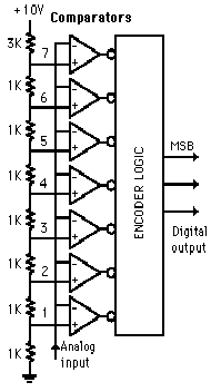
Illustrated is a 3-bit flash ADC with resolution 1 volt (after Tocci). The resistor net and comparators provide an input to the combinational logic circuit, so the conversion time is just the propagation delay through the network - it is not limited by the clock rate or some convergence sequence. It is the fastest type of ADC available, but requires a comparator for each value of output (63 for 6-bit, 255 for 8-bit, etc.) Such ADCs are available in IC form up to 8-bit and 10-bit flash ADCs (1023 comparators) are planned. The encoder logic executes a truth table to convert the ladder of inputs to the binary number output
To calculate the resolution of the ADC ...
The ADC below detects four different input levels
The resolution is Vref / 4
An 8 bit ADC can resolve 28 levels = 256 levels so the resolution is Vref / 256
To calculate the number of comparators (or exclusive OR gates) needed ...
2N - 1 comparators are needed where N is the number of bits in the output.
In the example below, there is a two bit output so 22 - 1 = 3 comparators needed.
For a four bit converter, 24 - 1 = 15 comparators needed.
For an 8 bit converter, 28 - 1 = 255 comparators needed. (hard to implement)
For a 16 bit converter, 216 - 1 = 65535 comparators needed. (Some CPU processors have millions of gates so this is entirely possible.)

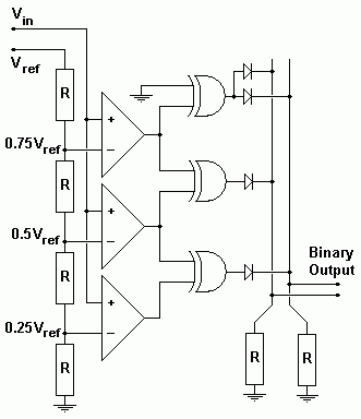
This is a two bit flash ADC (not very useful!) 8 or 16 bits would be much more use but also very much more complex.
The circuit above has three comparators.
Each comparator is fed a proportion of the reference voltage from Vref.
If the input voltage (Vin) is too low, all the comparators will be turned off.
If Vin is a little higher, only the bottom comparator will turn on.
If Vin is a little high still, the bottom two comparators will turn on.
If Vin is high enough, all the comparators will turn on.
If all the comparators are off, the output will be 0 0. This is zero in binary.
If the bottom comparator is on, the output will be 0 1. This is one in binary.
If the bottom two comparators are on, the output will be 1 0. This is two in binary.
If all the comparators are on, the output will be 1 1. This is three in binary.
Adding extra bits is simple. More comparators are needed and the output logic gets more complex too.
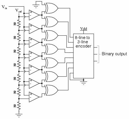
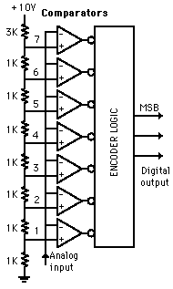
Also called the parallel A/D converter, this circuit is the simplest to understand. It is formed of a series of comparators, each one comparing the input signal to a unique reference voltage. The comparator outputs connect to the inputs of a priority encoder circuit, which then produces a binary output. The following illustration shows a 3-bit flash ADC circuit:
Vref is a stable reference voltage provided by a precision voltage regulator as part of the converter circuit, not shown in the schematic. As the analog input voltage exceeds the reference voltage at each comparator, the comparator outputs will sequentially saturate to a high state. The priority encoder generates a binary number based on the highest-order active input, ignoring all other active inputs.
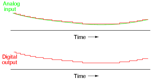
When operated, the flash ADC produces an output that looks something like this:
Due to the nature of the sequential comparator output states (each comparator saturating "high" in sequence from lowest to highest), the same "highest-order-input selection" effect may be realized through a set of Exclusive-OR gates, allowing the use of a simpl encoder:
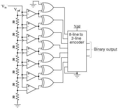
And, of course, the encoder circuit itself can be made from a matrix of diodes, demonstrating just how simply this converter design may be constructed:
While there are standard ICs that will perform the 8 line to 3 bit encoding (e.g. 74HC148) it is a useful exercise to consider how this could be achieved using normal logic gates.
The complete output is shown in the truth table below.
|
|
1 |
2 |
3 |
4 |
5 |
6 |
7 |
|
D0 |
D1 |
D2 |
|
|
0 |
0 |
0 |
0 |
0 |
0 |
0 |
|
0 |
0 |
0 |
|
|
1 |
0 |
0 |
0 |
0 |
0 |
0 |
|
1 |
0 |
0 |
|
|
1 |
1 |
0 |
0 |
0 |
0 |
0 |
|
0 |
1 |
0 |
|
|
1 |
1 |
1 |
0 |
0 |
0 |
0 |
|
1 |
1 |
0 |
|
|
1 |
1 |
1 |
1 |
0 |
0 |
0 |
|
0 |
0 |
1 |
|
|
1 |
1 |
1 |
1 |
1 |
0 |
0 |
|
1 |
0 |
1 |
|
|
1 |
1 |
1 |
1 |
1 |
1 |
0 |
|
0 |
1 |
1 |
|
|
1 |
1 |
1 |
1 |
1 |
1 |
1 |
|
1 |
1 |
1 |
|
|
|
|
|
|
|
|
|
|
|
|
|
Each output needs its own encoder. Consider D0. It needs to be logic 1 when:
Op-amp 7 output is logic 1,
Op-amp 5 output is logic 1 and op-amp 6 output is logic 0,
Op-amp 3 output is logic 1 and op-amp 4 output is logic 0,
Op-amp 1 output is logic 1 and op-amp 2 output is logic 0,
So a logic circuit for D0 is
It is a useful exercise to devise an encoding circuit for D1 and D2.
Multi-bit flash ADCs would have their encoders fabricated from Field Programmable Gate Arrays (FPGA). These are integrated circuits consisting of a very large numbers of logic gates which can be programmed by applying voltages to produce very complex logic systems.
Multi-bit flash ADCs are very expensive because of the requirement for many comparators and identical resistors. A 12 bit encoder requires 212 -1 (4095) comparators, each with a precision of at least 1 part in 4096 (i.e. 0.025%) or better.
Often such precision is needed. A -10 to 110C thermometer read to 0.1C requires a precision of 1 part in 1200, requiring at least an 11 bits ADC.
Note, if a 10 volt system is being used, a precision of 1 part in 1000 (i.e. 10 bits) corresponds to a signal voltage change of just 10mV. A 16 bit, 10V system is sensitive to signal changes of just 160V!
Electrical noise is a serious problem in ADCs since the logic circuit generates many transient electrical signals as the various logic gates switch. It is important to ensure that the input signal is kept away from the digital output. Correct use of the separate analogue and digital grounds on ADCs is vital to minimise problems with noise.
Merits of flash ADCs and Digital Ramp ADCs
The various advantages and disadvantages of Flash and Digital Ramp ADCs has already been considered in their respective sections. They are summarised in the table below.
|
|
FLASH ADC |
DIGITAL RAMP ADC |
|
COST |
Very expensive owing to the large number of comparators and identical resistors needed. |
Cheap. Can be implemented with a DAC and a comparator. |
|
SPEED |
Extremely fast especially when made with high speed comparators e.g. LM311. |
Slow to very slow. Only suitable for relatively slow changes in the analogue input. |
|
POWER CONSUMPTION |
High because of all of the comparators. |
Generally low. |
|
APPLICATIONS |
Digitisation of video and high quality audio signals |
Multi meters and Environmental monitors. |
Connecting an ADC to Microprocessor System
The block diagram of a generic ADC is shown below.
To control an ADC, a processor needs to have one-bit write lines going to the Start Conversion (SC) and the Output Enable (OE) terminals. It also needs a one-bit read line going to the End of Conversion (EoC) line and a multi-bit (8, 12 or 16) read port. The conversion process begins with the processor writing a logic 0 to the Start Conversion terminal and then monitoring the EoC terminal. When the ADC has finished the conversion, it sets EoC to logic 1. This tells the processor that the data in the data latch is valid and so the processor can write a logic 0 to the Output Enable terminal and then read the data into the port. The whole process can then be repeated as necessary.
This is shown diagrammatically below in the timing diagram.
Not only is the flash converter the simplest in terms of operational theory, but it is the most efficient of the ADC technologies in terms of speed, being limited only in comparator and gate propagation delays. Unfortunately, it is the most component-intensive for any given number of output bits. This three-bit flash ADC requires seven comparators. A four-bit version would require 15 comparators. With each additional output bit, the number of required comparators doubles. Considering that eight bits is generally considered the minimum necessary for any practical ADC (255 comparators needed!), the flash methodology quickly shows its weakness.
An additional advantage of the flash converter, often overlooked, is the ability for it to produce a non-linear output. With equal-value resistors in the reference voltage divider network, each successive binary count represents the same amount of analog signal increase, providing a proportional response. For special applications, however, the resistor values in the divider network may be made non-equal. This gives the ADC a custom, nonlinear response to the analog input signal. No other ADC design is able to grant this signal-conditioning behaviour with just a few component value changes.
Optical Shaft Encoder
A rotary encoder, also called a shaft encoder, is an electro-mechanical device that converts the angular position or motion of a shaft or axle to an analog or digital code.
There are two main types: absolute and incremental (relative). The output of absolute encoders indicates the current position of the shaft, making them angle transducers. The output of incremental encoders provides information about the motion of the shaft, which is typically further processed elsewhere into information such as speed, distance, RPM and position.
Rotary encoders are used in many applications that require precise shaft unlimited rotation—including industrial controls, robotics, special purpose photographic lenses,[1] computer input devices (such as optomechanical mice and trackballs), controlled stress rheometers, and rotating radar platforms.

![]()
Rotary encoder for angle-measuring devices marked in 3-bit binary. The inner ring corresponds to Contact 1 in the table. Black sectors are "on". Zero degrees is on the right-hand side, with angle increasing counterclockwise.
An example of a binary code, in an extremely simplified encoder with only three contacts, is shown below.
|
Standard Binary Encoding |
|
|||
|
Sector |
Contact 1 |
Contact 2 |
Contact 3 |
|
|
0 |
off |
off |
off |
|
|
1 |
off |
off |
ON |
|
|
2 |
off |
ON |
off |
|
|
3 |
off |
ON |
ON |
|
|
4 |
ON |
off |
off |
|
|
5 |
ON |
off |
ON |
|
|
6 |
ON |
ON |
off |
|
|
7 |
ON |
ON |
ON |
|
In general, where there are n contacts, the number of distinct positions of the shaft is 2n. In this example, n is 3, so there are 2³ or 8 positions.
In the above example, the contacts produce a standard binary count as the disc rotates. However, this has the drawback that if the disc stops between two adjacent sectors, or the contacts are not perfectly aligned, it can be impossible to determine the angle of the shaft. To illustrate this problem, consider what happens when the shaft angle changes from 179.9° to 180.1° (from sector 3 to sector 4). At some instant, according to the above table, the contact pattern changes from off-on-on to on-off-off. However, this is not what happens in reality. In a practical device, the contacts are never perfectly aligned, so each switches at a different moment. If contact 1 switches first, followed by contact 3 and then contact 2, for example, the actual sequence of codes is:
off-on-on (starting position)
on-on-on (first, contact 1 switches on)
on-on-off (next, contact 3 switches off)
on-off-off (finally, contact 2 switches off)
Now look at the sectors corresponding to these codes in the table. In order, they are 3, 7, 6 and then 4. So, from the sequence of codes produced, the shaft appears to have jumped from sector 3 to sector 7, then gone backwards to sector 6, then backwards again to sector 4, which is where we expected to find it. In many situations, this behaviour is undesirable and could cause the system to fail. For example, if the encoder were used in a robot arm, the controller would think that the arm was in the wrong position, and try to correct the error by turning it through 180°, perhaps causing damage to the arm.
Gray Code
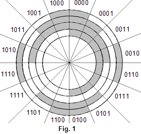
To track a rotating shaft in robot,
machinery, or CNC
machine, we have to use shaft optical encoder. There are two type of
shaft optical encoder, Incremental Encoder and Absolute
Encoder.
Absolute encoder has a binary coded disk - same as
the one shown in fig.1 - on a rotating shaft, white sections of
the disk in fig.1 are transparent while the grey sections are opaque.
An infrared emitter
is mounted on one side of each track, and an infrared receiver
("phototransistor")
is mounted on the other side of each track.
Outputs from the
four infrared receivers will produce on of the gray
code shown below, the disk will rotate when the shaft
rotates, as a result; the output grey code will vary. Each code
represents an absolute angular position of the shaft in its
rotation.
Disk in fig.1 is divided into 16 parts, as a result;
the position of the shaft can be determined to the nearest 22.5o
("360/16"). If the system requires more accuracy, designer
can use 8 bit disk which will make the result to the nearest 1.4o
("360/256")
What is Gray Code?
|
Decimal |
Binary 0000 |
Gray
Code |
Gray code is another binary code, just like BCD
code ("Binary Coded Decimal"), its play a big role in
automation, since it is used for encoding rotating shafts position.
This code is similar to binary code, it has the same possible
combinations but it is arranged in a different order as shown in the
table at the right.
You can generate the equivalent gray code
for any decimal number by constructing a table similar to the one we
have at the right. The LSB
column starts with one 0 then a set two 1's and two 0's as you go
down. The second LSB column starts with two 0's then a set of four
1's and four 0's as you go down, and so on for the rest digits.
The
purpose of using Gray Code.
The main reason to use gray
code instead of regular binary code is to reduce the size of the
largest possible error in reading the shaft position to the value of
the LSB. If the disk
used straight binary code, the largest possible error would be the
value of the MSB.
To
understand this, look at the table and suppose that the disk has
moved from the position 7 to the position 8 and the encoder fails to
read the MSB changed
bit. If the disk used straight binary code, the output code would be
0000 which is equal to the position number 0 that is far 8 steps from
the real location! Otherwise, when the same error occurs and the disk
used the Gray Code the output code would be 0100, which is equal to
the position number 7 that is only one step far from the real
position.
In general, when the gray code is used for disk
encoding, and the detectors fails to detect the new bit value during
the transition, the resulting code will be always the code for the
previous position. As a result, the maximum error will be always the
value of the LSB!
|
|
Optoswitches
The following two sensors are simply a pair of conveniently packaged emitter diodes and phototransistors, used for special purposes.
Slotted Optoswitch
The slotted optoswitch is an infrared
emitter and a phototransistor, in a single package with a gap
between them. It is used to check if an object is blocking the gap
between them.

One
common application is for counting the rotation of a disk with a
slot. The beam is blocked unless the slot is in the gap.
Points
to watch: It is usually necessary to follow a slotted
optoswitch with a comparator
to produce a definite logic ‘1’ or ‘0’. Some
slotted optoswitches include extra logic and don’t need a
comparator.
Reflective Optoswitch

The reflective optoswitch is also an infrared emitter and a
phototransistor, in a single package. However, they are arranged at
an angle to each other, so that the phototransistor only receives
infrared from the emitter if it is reflected from a nearby object.
These types of optoswitch are used in conjunction with shaft
encoders.
So the device is used to check if a reflective or
bright object (such a metal or a white surface) is nearby
Points
to watch: It is necessary to follow a reflective optoswitch
with a comparator
to produce a definite logic ‘1’ or ‘0’.
Photodiodes and Optical Switches
The PN junctions in diodes and transistors are light-sensitive. Photons cause electron-hole pairs to be formed, producing a current that is directly proportional to the light intensity.
A photodiode diode takes advantage of this by having a transparent window through which light can enter. It is usually used in reverse bias and the leakage current increases in proportion to the amount of light falling on the diode.
Photodiodes are used in a wide range of electronic circuits ranging from accurate light measuring equipment to high speed optical counters.
A photo diode can be interfaced in several ways, three of which are shown below.
The simplest circuit (a) treats the photodiode as a current source, and loads it with a resistor to obtain Vout = i × R.
But the current is small (1 electron per photon!), and the high resistance of the circuit to get measurable voltages at low light levels means that measuring systems attached to the output must have very high resistance. The maximum value of Vout is about 0.6 volt.
To overcome this problem, an op- amp can be used, as in circuit (b), to provide current and to act as a buffer. R may be of the order of 10M. Still Vout = i × R.
Faster response, for the same sensitivity, can be achieved by using the photodiode with reverse bias, as in circuit (c). The same current is produced because these are intrinsic electron-hole pairs being created at the junction by the photons but the op-amp acts as a buffer.
Optical-Switches
A LED and photodiode pair is often used as a digital sensing device.
A suitable circuit is shown below.
They can be used either in a transmission or a reflection mode. Applications are widespread, including whole revolution counting, measurement of shaft rotation rate, speed measurement, etc. A typical example of each type of optical switch is shown below.
A slotted opto-switch can be used to detect the presence of an obstacle between the LED and photo-transistor so preventing the light from the LED reaching the photo-transistor.
Reflective opto-switches consist of the LED and a photo-transistor side by side. When a reflective obstacle is placed near to the switch, light from the LED is reflected back to the photo-transistor.
Older type computer mice contain two slotted optical switches for detecting the movement of the ball, one for left / right and the other for forwards / backwards.
Output Subsystems
Candidates should be able to:
describe the circuit for an 8-bit Digital to Analogue Converter, DAC, based on a summing amplifier and explain its operation;
describe uses of a DAC;
calculate component values for a DAC;
calculate the output voltage from a DAC;
describe the use and operation of multiplexed seven segment displays (LCD and LED);
describe the use and operation of multiplexed dot matrix displays;
describe the different types of stepper motor;
describe the use and operation of stepper motors;
describe the essential differences in operation between conventional motors and stepper motors.
8-bit DAC Based on a Summing Amplifier
A simple 8-bit Digital to Analogue Converter (DAC) can be constructed using an op-amp in a summing amplifier circuit.
A basic 4-bit DAC is shown on page 39 of the ELEC2 Support booklet. To convert it to an 8-bit DAC four additional input resistors need to be added as shown below.
R7 = Rf, R6 = 2Rf, R5 = 4Rf, R4 = 8Rf
R3 = 16Rf R2 = 32Rf R1 = 64Rf R0 = 128Rf
The point labelled P on the circuit is a virtual earth point. The logic inputs, are D0, D1, D2, D3, D4, D5, D6, D7, with D7 being the most significant bit. The logic inputs are either logic 0 (0V) or logic 1 (often +5V). When an input is logic 1, a current to pass through its input resistor (R0 – R7). These currents cannot pass into the op-amp because it has such a large input resistance and so must pass through Rf. This causes a voltage to appear across Rf so resulting in a negative output voltage from the first op-amp which is directly related to the digital number applied to the inputs. The second op-amp functions as a unity gain inverting amplifier, so that the DAC gives a positive output.
Such a simple DAC is unsuitable for accurate conversions since it has two main failings.
While the output voltage from a logic gate is nominally 5V, it does vary from output to output. The principle of operation of this type of DAC relies on all of the input voltages being exactly the same and so errors in conversion will occur.
The resistors have to be very accurate multiples of the feedback resistor, Rf. Such resistors would be difficult to manufacture and so expensive. For a DAC having a conversion error of less than 1% would require the resistors to be accurate to 0.1%, assuming that the input voltages were all the same. However, a demonstration circuit can be made from the following standard 5% resistor values:
R7 = Rf = 10k
R6 = 20k (10k + 10k)
R5 = 40k (39k + 1k)
R4 = 80k (68k + 12k)
R3 = 160k (150k + 10k)
R2 = 320k (220k + 100k)
R1 = 640k (560k + 82k)
R0 = 1280k (1.2M + 82k)
Commercial DACs are based on the R-2R network, which can provide conversion accuracy of less than 0.1% at sensible prices. Such DACs are outside the scope of this specification.
Calculating the Output Voltage from a DAC
To calculate the output voltage from a DAC, with the component values in the example above, requires the use of the summing amplifier formula. This is given on the data sheet with each question paper.
Assume that logic 1 is +5V and logic 0 is 0V.
Consider when the input to the DAC is the value 0xA2. This needs to be converted to its binary value 10100010.
Using the general summing amplifier formula
then
Since the second op-amp is a unity gain inverting amplifier, the output voltage for an input of 0xA2 is 6.33V
Interfacing to a DAC
A generic block diagram for a DAC is shown in the diagram below, which consists of a Data Latch and the summing amplifier (or R – 2R network). The conversion starts when the processor writes the data into the DAC's latch using the Enable line (EN). The DAC produces an analogue output from the data and the output remains valid until the next byte of data is written to the DAC's latch.
The timing diagram for the conversion process is shown below.
7-Segment LED Displays
A 7-segment display consists of an array of LEDs arranged as in the diagram opposite.
The bars
of LEDs are designated with letters so that each bar can be referred
to in circuits, dp referring to the decimal point. To reduce the
number of connections to a seven segment display, either all of the
anodes of the LEDs are connected together, forming a
common
anode display, or the cathodes are joined forming a common
cathode display.
With a common anode displays, the common anodes of the LEDs are connected to the positive power supply line. The cathodes are then taken to 0V by the driving circuit to make the LEDs light. The 7447 IC will operate a common anode display and convert a binary input from 0 to 9 to the correct output on the display. This IC will supply (sink) up to 40mA per segment.
With the common cathode displays, the cathodes are connected to 0V. The anodes of the LEDs are then taken high by the driving circuit to illuminate the LEDs. The 4511 IC will operate a common cathode display and convert a binary input from 0 to 9 to the correct output on the display. This IC will supply (source) up to 25mA per segment.
Many
microcontrollers will also sink and source up to 25mA from their
output ports and so can directly operate
7-segment LED displays,
as shown in the diagram opposite for a common anode display.
In an attempt to save on components it might be thought that all of the LED series resistors could be replaced with one 220Ω resistor. If this is done then the brightness of the display would vary with the number of segments lit, which would be unsatisfactory.
In order to light the required LEDs to produce numbers it is simply a case of calculating what number to send to the output port. E.g. the number 1 requires that elements b and c are lit and the rest are switched off. Since the circuit above is common anode, D1 and D2 must be logic 0 and all of the others, logic 1. So the binary number that must be sent to the output port is 11111001 (0xFA). To produce the number 0, all of the bits from D0 to D5 must be at logic 0, with D6 and D7 at logic 1. I.e. the binary number 11000000 (0xC0) must be sent to the output port.
It is a useful exercise to work out what numbers must be outputted to display the other numbers. It is also useful to devise outputs to display the characters up to 15 in hexadecimal.
Multiplexed 7-Segment LED Displays
Nearly all measuring equipment needs more than one 7-segment display for its output. With the basic circuits, each 7-segment display will need its own decoder/driver IC, current limiting resistors etc leading to a high component count. To reduce the component count a technique known as Multiplexing is used, whereby each display is powered in turn and the rest of the time it is switched off. So long as this process is repeated fast enough, the persistence of vision of the eye, approximately 50ms, will make it appear as if all of the displays are lit. In this way, only one decoder driver IC is required plus a transistor switch for each display. It also means that a microcontroller with two 8-bit output ports could directly drive up to eight 7-segment displays.
The diagram below shows a possible arrangement for four common cathode displays.
All of the segment letters are connected in parallel giving just one connection for all of the ‘a’, one for ‘b’ etc through to one for ‘dp’. These are connected to PORTA of a microcontroller.
The common cathode of each display connects to a transistor switch, so that each display can be switched on in turn. These are controlled by PORTB.
In this example, each display is only switched on for 25% of the time and so will only appear to be 25% as bright as if the display was not multiplexed. It is excessive heat that damages LED displays, so if the overall power dissipation of each segment, averaged over one complete display cycle stays the same, the display segments will not be damaged. So this disadvantage can be overcome by passing four times the current to pass through each segment. So if the non multiplexed current per segment is 20mA, then 80mA could be allowed to pass without damage. Since most microcontrollers limit the output current from their ports to 25mA, it would be necessary to insert a high current driver between PORTA and the current limiting resistors to achieve the full brightness of the display.
Assuming that the current through each segment is 25mA, then if all of the segments of a display are switched on (including the decimal point), a current of 200mA will be passing through the cathode and the transistor switch. Care must therefore be taken when selecting the transistor switches to ensure that they can handle this maximum current.
Calculating The Resistor Values.
Assuming that the switching transistors have a current gain (Ic/Ib) of 100, then in order to have a maximum collector current of 200mA, it will be necessary for them to have a base current of 2mA. If the output voltage from PORTB is 5V and the base-emitter voltage of the transistor is 0.7V, then the voltage across the base resistor will be 4.3V and so the base resistor will be 4.3 / 0.002 = 2150Ω. The nearest suitable preferred value for this will be 2kΩ,
though a slightly lower value will help ensure that the transistor is saturated (fully switched on) and so dissipating minimum power.
Obviously, the switching transistors could be replaced with MOSFETs and then these resistors could be eliminated as the gates of the MOSFETs can connect directly to PORTB.
To calculate the series resistors for the LEDs, it is necessary to look up in the display data sheets the forward voltage for each segment. For Red and Green displays, this will be approximately 2V. When a transistor is saturated, its collector voltage is approximately 0.2V. So if PORTA supplies 5V, the voltage across the LED series resistor is 5 – 2 – 0.2 = 2.8V. If the current per segment is 25mA then R = 2.8 / 0.25 = 112Ω, the nearest preferred value being 110Ω, though a 120Ω resistor is likely to work as well.
Controlling the display.
Each of the digits of the multiplexed display needs to be activated in turn.
To switch
on digit A, it is necessary to make D0 of PORTB a
logic 1 and D1, D2 and
D3 logic
0. This is achieved by writing 0x01 to PORTB.
Switching on digit B only, is achieved by writing 0x02 to PORTB.
Switching on digit C only, is achieved by writing 0x04 to PORT B.
Switching on digit D only, is achieved by writing 0x08 to PORT B.
To display 1 on digit A, it is necessary to power segments b and c, which are connected to D1 and D2 of PORTA in this example. So the value 0x06 must be written to PORTA.
To display 2 on digit B, bits D0, D1, D3, D4 and D6 must be logic 1 so the value 0x5B must be written to PORTA.
To display 3 on digit C, bits D0, D1, D2, D3 and D6 must be logic 1 so the value 0x4F must be written to PORTA.
To display 4 on digit D, bits D1, D2, D5, and D6 must be logic 1 so the value 0x66 must be written to PORTA.
So to show 1 2 3 4 on the multiplexed display, the microcontroller should write 0x06 to PORTA and 0x01 to PORTB to display 1 on digit A.
It should then pause for 10ms (or so) to allow the observer to see the digit.
Then it should write 0x5B to PORTA and 0x02 to PORTB to display 2 on digit B.
It should then pause again for 10ms (or so) to allow the observer to see the digit.
Then it should write 0x4F to PORTA and 0x04 to PORTB to display 3 on digit C.
It should then pause again for 10ms (or so) to allow the observer to see the digit.
Then it should write 0x66 to PORTA and 0x08 to PORTB to display 4 on digit D.
It should then pause again for 10ms (or so) to allow the observer to see the digit and then start again with digit A.
Possible assembler instructions for the microcontroller to do this are shown below.
// Set PORTA to be output
MOVW 0x00 // Move 0 into W
MOVWR TRISA // Move the contents of W to TRISA
// Set PORTB so that D0 to D3 are outputs
MOVW
0xX0 // Set less significant nibble to 0. The value of the
more
// significant nibble does not matter and so is shown as
an X
MOVWR TRISB // Move the contents of W to TRISB
loop1: // Label for the display loop
//Display 1 on digit A
MOVW 0x06 // Move 6 into W
MOVWR PORTA // Move the contents of W to PORTA
MOVW 0x01 // Move 1 into W
MOVWR PORTB // Move the contents of W to PORTB
CALL
delay // Call a subroutine, ‘delay’, which is
elsewhere in memory
// and which gives a delay of 10ms
//Display 2 on digit B
MOVW 0x5B // Move 0x5B into W
MOVWR PORTA // Move the contents of W to PORTA
MOVW 0x02 // Move 2 into W
MOVWR PORTB // Move the contents of W to PORTB
CALL
delay // Call a subroutine, ‘delay’, which is
elsewhere in memory
// and which gives a delay of 10ms
//Display 3 on digit C
MOVW 0x4F // Move 0x4F into W
MOVWR PORTA // Move the contents of W to PORTA
MOVW 0x04 // Move 4 into W
MOVWR PORTB // Move the contents of W to PORTB
CALL
delay // Call a subroutine, ‘delay’, which is
elsewhere in memory
// and which gives a delay of 10ms
//Display 4 on digit D
MOVW 0x66 // Move 0x66 into W
MOVWR PORTA // Move the contents of W to PORTA
MOVW 0x08 // Move 8 into W
MOVWR PORTB // Move the contents of W to PORTB
CALL
delay // Call a subroutine, ‘delay’, which is
elsewhere in memory
// and which gives a delay of 10ms
JMP loop1 // Go to the beginning of the display program and start again.
This program would continue to show the numbers 1, 2, 3, 4 on the display until the power was turned off or the microcontroller reset.
LCD Multiplexed Displays
LED displays have two main disadvantages; they consume significant power and are difficult to read in bright sunlight. They do have the advantages that they can be seen in the dark, switch quickly and are physically robust.
Liquid Crystal Displays, LCDs, are the exact opposite of LED displays; they consume little power and are easily read in bright light, but they are delicate, switch slowly and, to be read in the dark, they have to have a light behind them (back lit), which consumes power.
The first liquid crystal to be discovered was Cholesteryl benzoate.
The molecules possess strong dipoles and easily polarisable groups.
The electric dipole-dipole interactions between molecules give rise to intermolecular forces which align the molecules side by side with their long axes parallel.
There are three main types of liquid crystal materials, known as smetic, nematic and cholesteric, but it is mainly the nematic class of materials that are used in electronic displays. The molecules of this type arrange themselves with their long axis parallel to one another, but take up any position along their axes with respect to adjacent molecules, so that they exhibit a 'grain' but do not form layers.
A typical nematic liquid crystal display takes the form of flat panels which consist of two glass plates, each about 3mm thick, separated by a layer of liquid crystal material of thickness 0.025mm. The glass plates are hermetically sealed at their edges. The inside surfaces of the glass plates have deposited on them a transparent conducting layer in the form of the pattern to be displayed. This layer is often tin oxide which has been baked (sintered) onto the glass.
The long axis of liquid crystal molecules align themselves normally to the surface of the glass. When a voltage is applied, it has the effect of turning the molecules through a right angle so that the dipole axes are brought into line with the electric field. At the same time free negative and positive ions are drawn to the appropriate oppositely charged conducting surfaces and, while passing through the liquid locally, neutralise the field across the liquid in the sandwich. This results in small groups of molecules becoming randomly disorientated in the rest of the sandwich, so producing what appears to be a 'milky' or 'ground glass' effect.
Such liquid crystal displays are adequate for devices such as calculators but are inadequate for graphics display applications because of their limited viewing angle and colour stability. These problems are overcome to a large extent by the Twisted Nematic (TN) cell and the Super Twisted Nematic (STN) cell.
In both TN and STN displays the thin layer of liquid crystal molecules is sandwiched between two transparent plates coated with a polymer. The polymer surface is rubbed before assembly with a velvet cloth to put fine lines onto the polymer. These lines ensure that the liquid crystal molecules all point in one direction in the plane of the liquid crystal layer, with their axes parallel to the polymer. The lines on the top and bottom polymer surfaces are arranged at 90° so that the liquid crystal molecules also twist through 90° through the thickness of the liquid crystal film. The liquid crystal and transparent plate assembly is then sandwiched between two polarising filters with their planes of polarisation aligned to the liquid crystal molecules. Light is therefore able to pass through the arrangement.
When an electric field is applied across the liquid crystal cell, the liquid crystal molecules rotate so that their axes are normal to the polymer surface. The plane of polarisation of the light is no longer rotated by 90° and so no light is transmitted by the cell.
STN displays use a similar principle to the TN displays but use a larger angle of twist for the liquid crystals. The angle can be as large as 270o and results in a much improved contrast and viewing angle.
The largest market for LCDs is dot matrix module products integrating LCD glass and driver circuitry onto a single unit. STN colour graphics panels of up to 2000 x 1200 pixels are used in portable computers and LCD televisions. Thin film transistors are incorporated into the cell structure and colour is achieved by depositing red, green and blue filters onto the display front face in front of the pixels. Back lighting is provided by cold cathode fluorescent lamps (CCFLs) or LEDs.
Unlike other display technologies that respond to peak or average voltage and current, LCDs are sensitive to the rms voltage between the backplane and given segment location.
Any direct bias voltage across this junction would cause an irreversible electrochemical action that would shorten the life of the display. A typical LCD driving signal is shown below.
The backplane signal is simply a symmetrical square wave. The individual segment outputs are also square waves, either in phase with the backplane for an ‘off’ segment or out of phase for an ‘on’ segment. This causes a rms voltage of zero for an ‘off’ segment and a rms voltage of ‘Vs’ for an ‘on’ segment.
Single digit LCDs are not made – they are usually produced with three or more digits multiplexed together. As a result of ensuring that there is never a direct bias voltage across a LCD segment, it is much more complex to drive a multiplexed LCD than a LED display and it is usually done by dedicated ICs.
Some LCDs
are stated as being 3½ or 4½ digit displays. The
‘half’ refers to the leading digit which can be a 0 or a
1, so giving a maximum display of 1999 for the 3½ digit
display or
19999 for the 4½ digit display.
LED Dot Matrix Displays
The standard seven segment display is limiting in the way in which it is able to display numbers, characters and symbols. A popular alternative is the LED dot matrix display. This consists of 35 LEDs arranged in five columns and seven rows as shown in the diagram below.
Dot matrix displays are available with the anodes of the LEDs connected to form the columns or the cathodes connected to form the columns. The diagram below shows the LEDs wired with the cathodes connected to the column lines and the anodes connected to the row lines. So to light an LED a column line must go to logic 0 and a row must go to logic 1.
To produce characters on the display it is necessary to continuously set each of the column lines to logic 0 in turn while setting the appropriate row lines to logic 1. Consider creating the character, A, as shown below on the display diagram below.
When C0 is at logic 0 and all of the other columns are at logic 1, rows R2, R3, R4, R5 and R6 must be at logic 1 with all of the other rows at logic 0. The display then looks as in the diagram below.
C1 is then set to logic 0 with the other columns at logic 1 and rows R1 and R3 are set to logic 1 with the other rows set to logic 0. The display then looks as below.
Column C2 is then set to logic 0 and rows R0 and R3 to logic 1. The display then becomes as below.
Column C3 is then set to logic 0 and rows R1 and R3 to logic 1. The display then becomes as below.
Column C4 is then set to logic 0 and rows R3, R4, R5 and R6 to logic 1. The display then becomes as below.
If this process occurs rapidly enough then the eye perceives this as the character
While this type of display offers considerable flexibility in the size and form of the characters displayed, it does suffer from two serious disadvantages.
The scanning process by which each column is activated in turn must be fast and continuous. This can take up significant processing time from the control system.
For a five column display, the LEDs are only lit for 20% of the display time and so they will only be at 20% of their normal brightness. This disadvantage can be reduced by passing significantly more current through the LEDs. This does not harm the LEDs so long as the mean current is within the normal operating parameters.
The circuit below shows how a LED dot matrix display can be operated from a microcontroller.
All of the same considerations that were made for the multiplexed 7-segment displays apply to the multiplexed dot matrix display, including the resistor calculations.
So to display the character
the following numbers must be sent to the interface:
|
Column |
0 |
1 |
2 |
3 |
4 |
|
PORTA |
0x7C |
0x0A |
0x09 |
0x0A |
0x7C |
|
PORTB |
0x01 |
0x02 |
0x04 |
0x08 |
0x10 |
|
|
|
|
|
|
|
There should be a small pause between each set of column and row numbers being sent to the interface to enable the eye to register which LEDs are illuminated.
Assembler instructions that will display the character are given below.
// Set PORTA to be output
MOVW 0x00 // Move 0 into W
MOVWR TRISA // Move the contents of W to TRISA
// Set PORTB so that D0 to D4 are outputs
MOVW 0x00 // Move 0x00 into W.
MOVWR TRISB // Move the contents of W to TRISB
loop1: // Label for the display loop
//Display the first column
MOVW 0x7C // Move 0x7C into W
MOVWR PORTA // Move the contents of W to PORTA
MOVW 0x01 // Move 1 into W
MOVWR PORTB // Move the contents of W to PORTB
CALL delay // Call a subroutine, delay which is elsewhere in memory and // which gives a delay of 5ms
//Display the second column
MOVW 0x0A // Move 0x0A into W
MOVWR PORTA // Move the contents of W to PORTA
MOVW 0x02 // Move 2 into W
MOVWR PORTB // Move the contents of W to PORTB
CALL delay // Call a subroutine, delay which is elsewhere in memory and // which gives a delay of 5ms
//Display the third column
MOVW 0x09 // Move 0x09 into W
MOVWR PORTA // Move the contents of W to PORTA
MOVW 0x04 // Move 4 into W
MOVWR PORTB // Move the contents of W to PORTB
CALL delay // Call a subroutine, delay which is elsewhere in memory and // which gives a delay of 5ms
//Display the fourth column
MOVW 0x0A // Move 0x0A into W
MOVWR PORTA // Move the contents of W to PORTA
MOVW 0x08 // Move 8 into W
MOVWR PORTB // Move the contents of W to PORTB
CALL delay // Call a subroutine, delay which is elsewhere in memory and // which gives a delay of 5ms
//Display the fifth column
MOVW 0x7C // Move 0x7C into W
MOVWR PORTA // Move the contents of W to PORTA
MOVW 0x10 // Move 0x10 into W
MOVWR PORTB // Move the contents of W to PORTB
CALL delay // Call a subroutine, delay which is elsewhere in memory and // which gives a delay of 5ms
JMP loop1 // Go to the beginning of the display program and start again.
This program would continue to show the letter A on the display until the power was turned off or the microcontroller reset.
Stepper Motor
Controlling the speed and position of a motor with a slotted disk or a shaft encoder is complex and can be inaccurate due to the overshoot and settling time of the motor. An alternative and superior device in low power applications is the stepper motor. Stepper motors are commonly used in all kinds of equipment where accurate positioning is essential, particularly computer controlled equipment e.g. printers, scanners, disk drives, robot arms etc. Their power output ranges from a few micro-watts when used to drive the hands of an analogue quartz watch up to about 1kW for industrial applications. Apart from the accurate positioning of the shaft, stepper motors also have the advantage that they hold the shaft firmly in place while they are stopped. However, they are inefficient in changing electrical power to mechanical power.
There are two main types of stepper motor, permanent magnet and variable reluctance. These two distinct types can also be combined into a hybrid motor which functions in a similar way to permanent magnet type but offers greater angular resolution. Without any power applied, permanent magnet motors tend to feel ‘lumpy’ as they are twisted by hand, while variable reluctance motors almost spin freely.
Stepper motors come in a wide range of angular resolution. The coarsest motors typically turn 90 degrees per step, while high resolution permanent magnet motors are commonly able to handle 1.8 or even 0.72 degrees per step. With an appropriate controller, most permanent magnet and hybrid motors can be run in half-steps, and some controllers can handle smaller fractional steps or microsteps.
Variable Reluctance Stepper Motor.
This type of stepper motor has been around for a long time. It is probably the easiest to understand from a structural point of view. This type of motor consists of a soft iron multi-toothed rotor and a wound stator. The diagram below shows a cross section of a typical variable reluctance stepper motor consisting of three coils and a 4 toothed rotor. When the stator windings are energized with direct current the poles become magnetized. Rotation occurs when the rotor teeth are attracted to the energised stator poles.
The diagram below shows the rotor turning 30° as the coils are energized in turn 1, 2, 3 and 1, giving a total rotation of 90°.
This is an example of a unipolar motor, since the current only flows in one direction through the coils. To make the motor rotate in the other direction then the coils are energised in the opposite order, i.e. 3, 2, 1 and 3.
Permanent Magnet Stepper Motor
The permanent magnet stepper motor is a low cost and low resolution type motor with typical step angles of 1.8° to 30°. As the name implies, these motors have permanent magnets added to the motor structure. The rotor is magnetized with alternating north and south poles situated in a straight line parallel to the rotor shaft. These magnetized rotor poles provide an increased magnetic flux intensity and because of this the permanent magnet stepper motor exhibits improved torque characteristics when compared with the variable reluctance type.
The diagram below shows a unipolar permanent magnet stepper motor consisting of two coils which are centre tapped. Coil 1 is distributed between the top and bottom stator pole, while coil 2 is distributed between the left and right motor poles. The rotor is a permanent magnet with 6 poles, 3 south and 3 north, arranged around its circumference.
As shown in the diagram, the current flowing from the centre tap of winding 1 to terminal a causes the top stator pole to be a south pole while the bottom stator pole is a north pole. This attracts the rotor into the position shown. If the power to winding 1 is removed and winding 2 is energised, the rotor will turn 30 degrees, or one step.
It is useful to verify that if two more sets of coils were added at an angle of 45° to the existing coils then the step angle would be reduced to 15°.
The diagram below shows the rotor turning 30° as the coils are energized in turn 1a, 2a, 1b and 2b, giving a rotation of 90°.
This is another example of a unipolar motor, since the current only flows in one direction through the coils. To make the motor rotate in the other direction then the coils are energised in the opposite order, i.e. 2b, 1b, 2a and 1a.
Hybrid Stepper Motor
The hybrid stepper motor is more expensive than the permanent stepper motor but provides better performance with respect to step resolution, torque and speed. The typical step angles for the hybrid stepper motor range from 7.5° to 0.9°. The hybrid stepper motor combines the best features of both the permanent magnet and the variable reluctance type stepper motors. The rotor is multi-toothed like the variable reluctance motor and contains an axially magnetized concentric magnet around its shaft. The teeth on the rotor provide an even better path which helps guide the magnetic flux to preferred locations in the air gap. This further increases the holding and dynamic torque characteristics of the motor when compared with both the variable reluctance and permanent magnet types.
In the simplified diagram above, the pole pieces of the coils each have two teeth at an angle of 30° to each other. The pole pieces for each part of each coil are off set from each other by 7.5°. The rotor consists of a magnetic cylinder with North poles on the top and South poles on the bottom, as shown above.
The diagrams below show how the rotor will rotate 7.5° as the coils are energized in turn giving a total rotation of 22.5°.
The two most commonly used types of stepper motors are the permanent magnet and the hybrid types.
For both permanent magnet and variable reluctance stepping motors, if just one winding of the motor is energised, the rotor (under no load) will snap to a fixed angle and then hold that angle until the torque exceeds the holding torque of the motor, at which point, the rotor will turn, trying to hold at each successive equilibrium point.
Bipolar Motors
Bipolar permanent magnet and hybrid motors are constructed with exactly the same mechanism as is used on unipolar motors, but the two windings are wired more simply, with no centre taps. Thus, the motor itself is simpler but the drive circuitry needed to reverse the polarity of each pair of motor poles is more complex. The diagram below shows how such a motor is wired, while the motor cross section shown here is exactly the same as the cross section as the unipolar permanent magnet stepper motor.
The drive circuitry for such a motor requires an H-bridge control circuit for each coil which allows the polarity of the power applied to each end of each winding to be controlled independently. The H-bridge circuit is fully described in the section on Interfacing.
To make the motor rotate, the coils have to be powered as in the table below.
|
1a |
+ |
|
– |
|
|
1b |
– |
|
+ |
|
|
2a |
|
+ |
|
– |
|
2b |
|
– |
|
+ |
This will make it rotate 90°, as shown in the diagram below.
Controlling a Stepper Motor.
A stepper motor can readily be controlled by a microcontroller. However, the current needed to pass through the coils of the motor is much larger than the microcontroller PORT outputs can supply and so they need to be buffered. This can either be done using a dedicated driver IC e.g. the ULN2803A, which contains eight high current, open collector transistors, or by using discrete MOSFETs.
The circuit diagram below shows such an arrangement of MOSFETs controlling a unipolar stepper motor. Note the four protection diodes for the MOSFETs.
An assembler program to control the motor is shown below. In this program:-
bit 6 of PORTB determines the direction,
bit 7 of PORTB controls start/stop and
bits 0 to 3 determine the speed.
The stepper motor is controlled by bits 0 to 3 of PORTA
// Set PORTA to be output
MOVW 0x00 // Move 0 into W
MOVWR TRISA // Move the contents of W to TRISA
// Set PORTB to be input
MOVW 0xFF // Move 0xFF into W.
MOVWR TRISB // Move the contents of W to TRISB
// Start or stop?
start: // Label for the start of the control program
MOVRW PORTB // Move the contents of PORTB to W
ANDW 0x80 // Mask all but bit 7
JPZ start // If bit 7 is zero, ie stop, then check again
// Check direction of rotation
MOVRW PORTB // Move the contents of PORTB to W
ANDW 0x40 // Mask all but bit 6
JPZ anticlockwise // If bit 6 is zero then anticlockwise, if 1 clockwise.
clockwise: // Label for the clockwise code
MOVW 0x01 // Move 1 into W
MOVWR PORTA // Move the contents of W to PORTA
CALL delay // Call the delay subroutine.
MOVW 0x02 // Move 2 into W
MOVWR PORTA // Move the contents of W to PORTA
CALL delay // Call the delay subroutine.
MOVW 0x04 // Move 4 into W
MOVWR PORTA // Move the contents of W to PORTA
CALL delay // Call the delay subroutine.
MOVW 0x08 // Move 8 into W
MOVWR PORTA // Move the contents of W to PORTA
CALL delay // Call the delay subroutine.
JMP start // Go to the start of the program to check start/stop and direction
anticlockwise: // Label for the anticlockwise code
MOVW 0x08 // Move 8 into W
MOVWR PORTA // Move the contents of W to PORTA
CALL delay // Call the delay subroutine.
MOVW 0x04 // Move 4 into W
MOVWR PORTA // Move the contents of W to PORTA
CALL delay // Call the delay subroutine.
MOVW 0x02 // Move 2 into W
MOVWR PORTA // Move the contents of W to PORTA
CALL delay // Call the delay subroutine.
MOVW 0x01 // Move 1 into W
MOVWR PORTA // Move the contents of W to PORTA
CALL delay // Call the delay subroutine.
JMP start // Go to the start of the program to check start/stop and direction
delay: // Label for the delay subroutine
MOVRW PORTB // Move the contents of PORTB to W
ANDW 0x0F // Mask bits 4 to 7
delay1: // Label for the start of the delay loop
CALL
delay2 // Subroutine call to another subroutine generating a
delay
// of 2ms. The delay2 subroutine is elsewhere in the
memory // but not shown in this example.
SUBW 0x01 // Subtract 1 from W. This decrements the value that was set as // the speed for the motor.
JPZ last // If it is zero then jump to the end of the subroutine
JMP delay1 // Repeat the delay loop.
last: // label for the end of the subroutine
RET // Return from delay subroutine.
Comparison of Conventional and Stepper Motors
|
|
Conventional |
Stepper |
|
Connections |
Usually two but there can be four if the field coils are separate to the rotor coils. |
Often four or six connections but there can be more depending on the number of field coils |
|
Speed |
Up to 30,000 rpm |
Up to a few hundred rpm |
|
Control |
Can be controlled by an on/off switch. |
Needs an electronic control circuit. |
|
Efficiency |
Can be as high as 90% |
Very low (10 – 40%) as most of the power is dissipated as heat. |
|
Starting torque |
Starts high and is reasonably constant over a wide range of speeds. |
Starts high but decreases with speed of rotation. |
|
Holding torque |
There is no stationary holding torque for most motors, since no power is supplied if the motor is stationary. |
Starts high but decreases with speed of rotation |
|
Power |
Up to several megawatts |
Up to several hundred watts. |
|
Accuracy of rotation |
No accuracy at all unless used with either a servo arrangement or a shaft encoder |
3 – 5% of a step on the overall angle turned through. |
|
|
|
|
Interfacing Subsystems
Candidates should be able to:
describe the use of tri-state buffers;
describe the use of data latches;
describe how data latches can be constructed from D-type flip-flops;
recall the circuits for inverting Schmitt triggers and describe their operation;
calculate the switching levels for inverting Schmitt triggers;
explain how a Schmitt trigger can be used to regenerate a noisy input signal;
describe the circuits needed to drive multiplexed displays (LCD and LED);
recall the circuit for an H-bridge driver and describe its use and operation;
describe the circuits needed to drive both conventional and stepper motors.
Tri-state Buffers.
A tri-state buffer has three possible output states, logic 0, logic 1 and a high impedance state.
For data
to be read by a control system, it needs to be placed onto the data
bus. With all of the other data signals flowing along the data bus
it is essential that the data to be read is only placed onto the data
bus at precisely the time that the processor wants to read the
data.
A tri-state buffer is therefore needed to link the external
data to the data bus. The high impedance state of a tri-state buffer
is controlled by a pin labelled output enable, (OE).
A single bit tri-state buffer can be considered to be the circuit diagram below:
In many
ICs this is active low, i.e. when the (OE) pin is logic 1, their
outputs have a high impedance. When the (OE) pin is logic 0, the
output is enabled to either logic 0 or 1. Many devices for use on
computer buses have tri-state drivers built into them,
e.g.
analogue to digital converters, (ADCs), memory devices etc.
A suitable circuit is shown in the diagram below.
For the processor to be able to access the external data, it must supply the correct address for the input port and also set the R/W control line to logic 1. These two signals, when NANDed together, make the , (OE), low, which connects the external data to the data bus via the tristate buffer.
There are several ICs which can be used for the tri-state buffer for this application including the 74HC241 and the 74HC244 devices, both of which are 8-bit devices.
Data Latches
For data to be written from a control system to an output port, the processor sets the address of the port, sets the R/W control line to logic 0 and then place the data onto the data bus. The data will only remain on the data bus for one cycle of the clock, which for a processor operating with a 330MHz bus will only be 3ns! Since external devices usually respond slowly, they are likely to miss the data! It is therefore normal for the output port to consist of a latch, into which the data can be stored and the external device can then access it when it is ready. Such a circuit is shown below.
For data to be written from a control system, the processor will set the address of the port and set the R/W control line to logic 0. This will make the output of the AND gate logic 1 which enables the latch. The processor then place the data onto the data bus and then sets the R/W control line to logic 1. This locks the data into the latch, ready for the external device to use when ready.
Page 20 of the ELEC2 Support Booklet describes how a 4-bit Data Latch can be made from D-type flip-flops. This can easily be extended to make an 8-bit latch by using another four D-type flip-flops.
Because of the speed which many processors now operate, it is necessary to use high speed D-type flip-flops to capture the data, e.g. 74HC74 devices. An 8-bit latch would use four 74HC74s. This would occupy much space on a circuit board and so it is usually preferable to use an IC which contains a complete 8-bit latch e.g. the 74HC373 device.
A Schmitt trigger circuit can convert an analogue signal into a digital signal. You were introduced to a comparator circuit that will do this some time ago, but the difference is that where the comparator had just one threshold level, the Schmitt trigger has two threshold levels, one for rising signal levels and another for falling signal levels. The gap between the two threshold levels is called the hysteresis, and is brought about by the Schmitt trigger circuit using positive feedback.
Schmitt trigger circuits can either be obtained as a variation of some logic ICs or they can be designed using an op-amp. Most of this topic is concerned with designing Schmitt trigger circuits from op-amps.
If you look at the graphs of the behaviour of a Schmitt trigger circuit in operation compared with a comparator when operating from the same input signal, you will see the difference between them in terms of input/output behaviour.
Look at the comparator graph to see that the comparator output changes when the input signal crosses the single threshold level.
Compare this with the Schmitt trigger graph to see that the output only goes high when the upper threshold has been crossed, and then the lower threshold must be crossed before the output can return to a low level.
This is illustrated on the next page.
Analogue input
Threshold level
0V
Comparator output
Analogue input
Threshold level 1
Threshold level 2
0V
Comparator output
As you can see from the graphs, both circuits react to the analogue input signal, but produce outputs based on different threshold levels. Not much difference is evident so far. The difference really becomes obvious when a ‘noisy’ analogue signal is fed in to both circuits.
Analogue input
Threshold level
0V
Comparator output
Analogue input
Threshold level 1
Threshold level 2
0V
Comparator output
It can be seen that the Schmitt trigger circuit ‘cleans up’ the dirty signal; producing one clear on and one clear off signal from the analogue input signal.
An example of a system that depends on this response is the control circuit for streetlights, which must switch on at dusk and switch off at dawn. It would not be satisfactory to have street lighting flashing on and off repeatedly as dusk falls, maybe with clouds affecting the light level, as in the dirty analogue signal.
The action of having two threshold levels is very useful, giving a gap or hysteresis between the two levels, to give the system some noise immunity.
Schmitt trigger circuits are also used to regenerate digital signals sent over long communications links, as will be seen in the next Module. All the noise can be removed from the signal and the clean signal passed on to the next stage in the link. This enables us to have good quality audio and video communication around the world.
All the Schmitt trigger circuits that follow are made using op-amps. The simplest one just uses the op-amp IC alone. A key element in the circuit is positive feedback - this is what gives rise to the two threshold levels.
Many op-amps when connected to a ±12V supply produce maximum (saturated) outputs of ±10V. Generally, an op-amp will give an output voltage around 2-3V less than the power supply voltage. This output is fed back to the non-inverting input. This is what constitutes positive feedback and gives the different threshold levels, one when the output is at positive saturation and the other when the output is at negative saturation.
Examine the operation of this circuit:
VIN
VOUT
When the output of the circuit is +10V, VIN must exceed +10V before the output will change state to –10V (it is acting as a comparator). When the output of the circuit is –10V, the input must then go below –10V to trigger a return to +10V at the output.
This behaviour is best illustrated in an input/output graph:
VOUT
+10V
VIN
-10V +10V
-10V
This is an example of an inverting Schmitt trigger. Since the output is high when the input is low, as soon as the input rises above the higher threshold level (+10V), the output level falls to –10V and this is fed back to the non-inverting input, creating a lower threshold level. The input must then fall below the lower threshold level (-10V) before the output returns to +10V.
Rather unusually, this is generally done from output to input. Due to the saturated output voltage being known, this can be used together with the op-amp behaving as a simple comparator in calculating the two threshold levels, and so analysing the operation of a given circuit.
All of these circuits give out a high voltage when the input voltage goes low.
A voltage divider can be added to feedback a fraction of the saturated output voltage.
Assume all op-amps operate on a ±12V supply and give saturated outputs of ±10V.
VIN
VOUT
R1
R2
0V
If R1 = R2, then the voltage at X will be the voltage across R2, half of the 10V. So the threshold levels will be ±5V. This is illustrated by the input/output graph.
The input/output graph:
VOUT
+10V
VIN
-5V +5V
-10V
Any reasonable combination of R1 and R2 can be used to select any fraction of the output voltage to be used as threshold voltages.
Exercise:
If R1 = 39kW
And R2 = 1kW
Calculate the threshold levels if the saturated output voltages are ±10V.
and
These circuits give symmetric threshold levels (equal positive and negative threshold levels).
Draw an input/output graph for this circuit; the saturated levels are dotted in on the next page:
The input/output graph:
VOUT
+10V
VIN
-2 -1 0 1 2
-10V
An asymmetric inverting Schmitt trigger circuit
Note how the analysis of this circuit is made simpler by noting voltage levels at points in the circuit. These are noted underneath the respective points in the circuit and start from known reference points such as saturated output voltages and reference input voltages. All that is required is to calculate the voltage present on the non-inverting input of the op-amp. This will be the relevant threshold voltage level since the op-amp acts as a comparator.
As an example, let Vref = +4V.
VIN
VOUT
Vref = +4V
When VOUT 6V
= +10V
3V 3V
+4V +7V +10V
When VOUT -14V
= - 10V
7V 7V
+4V -3V -10V
So the two threshold levels are +7V and –3V, since these voltages are present on the non-inverting input for the two saturation output levels, and the op-amp acts as a comparator, testing the input, VIN against these levels.
Where the two resistors are unequal, use voltage divider theory to find the intermediate voltage.
‘Dot in’ the two threshold levels +7V and –3V.
‘Dot in’ the two output levels +10V and –10V.
Complete the diagram by inserting solid lines where needed. Note the inverting action.
VOUT
+10V
-3V +7V VIN
-10V
The input/output graph consists of a rectangle with two “tails”. For an inverting action, the tails should show a negative output for a positive input, and a positive output for a negative input. Overall, the graph should show a negative slope, i.e.;
Analyse the following inverting Schmitt trigger circuit. Assume the saturated output voltages are ±10V. Find the two threshold voltages and draw the input/output graph.
VIN
VOUT
Vref = +2V
When VOUT
= +10V
+10V
When VOUT
= - 10V
-10V
Threshold levels
Draw an input/output graph for this circuit; the saturated levels are dotted in.
VOUT
+10V
VIN
-10V
Other variations of inverting Schmitt trigger circuits
Diodes (and resistors) can be added to clamp the output voltage of the op-amp. This means that the forward and/or reverse voltage of the diodes can act to limit the output voltage to values less than the saturated values.
Examples:
Use of Zener diodes across the output circuit
VIN
VOUT
0V
The output voltage of this circuit always has one forward-biased Zener diode (=0.7V) and one reverse-biased Zener diode (whatever VZ is), which will pull the output voltage (and so affect the threshold voltages) down to VZ + 0.7V.
For example, two 4.7V Zener diodes would clamp the output voltage to ±5.4V and these would be the threshold voltages. If this circuit had a voltage divider as well, its effect would be calculated after considering any clamping action.
Draw an input/output graph for this circuit:
VOUT
VIN
Use of diodes and resistors across the output circuit
VIN
VOUT
0V
When the output at the op-amp is ±10V, the feedback voltage will be the Zener voltage if the resistor conducts less than 10 – 15 mA (check it). When the output of the op-amp is –10V, the feedback voltage is –0.7V as the Zener diode is now forward-biased.
Draw an input/output graph for this circuit:
VOUT
VIN
Use of diodes and resistors in the feedback chain
VIN
VOUT
Vref
When the output is ±10V, the diode is forward-biased, subtract 0.7V before you get to the right-hand side of the feedback resistor. Continue the analysis as normal.
When the output is –10V, the diode is reverse-biased and this effectively ‘switches off’ the feedback circuit. The non-inverting input voltage is then equal to Vref since no voltage is lost across the input resistor (no current is drawn by the non-inverting input).
Draw an input/output graph for this circuit if Vref is +2V:
VOUT
VIN
There are other versions of inverting Schmitt trigger circuits. Use these notes as a guide, and your knowledge of voltage dividers and diode behaviour. It is always best to analyse any Schmitt trigger circuit using basic concepts. VIN always connects to the inverting input of the op-amp in an inverting Schmitt trigger circuit.
Robotic Systems
Candidates should be able to:
describe the essential components of robotic systems sensors, actuators and control architectures;
describe the merits and suitability of different power sources;
design control algorithms for a robotic system to achieve a given objective;
describe the ability of such systems to sustain artificially intelligent behaviour through the use of artificial neural networks;
discuss the applications of robotic systems;
describe the social and economic impact of robotic systems;
describe possible future developments of robotic systems.
Robots
The word robot was introduced to the public by Czech writer Karel Capek in his play R.U.R. (Rossum's Universal Robots), published in 1920. The play begins in a factory that makes artificial people called robots, but they are closer to the modern ideas of androids, creatures that can be mistaken for humans. They are able to think for themselves, but seem happy to serve humans.
The word robotics which is used to describe this field of study, was coined (albeit accidentally) by the science fiction writer Isaac Asimov in his work the “Foundation Series” and in his “Three laws of Robotics”
There is no one definition of robot which satisfies everyone, and many people have their own.
The Robotics Institute of America (RIA) defines a robot is a "re-programmable multi-functional manipulator designed to move materials, parts, tools, or specialized devices through variable programmed motions for the performance of a variety of tasks".
The International Organization for Standardization gives a definition of robot in ISO 8373: "an automatically controlled, reprogrammable, multipurpose, manipulator programmable in three or more axes, which may be either fixed in place or mobile for use in industrial automation applications."
The range and types of robotic systems is continually developing and the table below shows some of the current types.
|
Domestic |
Floor cleaning e.g. CleanMate Lawn mower e.g. The Roomba, Robomow |
|
Industrial |
Welding, lifting, positioning etc e.g KUKA KR1000 titan |
|
Toys |
Roboraptor, Lego Mindstorms NXT |
|
Medical |
da Vinci surgical system |
|
Science |
Mars Rovers, Spirit and Opportunity |
|
Military |
Bomb disposal, e.g tEODor Reconnaissance, e.g. Asendro vehicle, Predator Drone remote aircraft Battlefield drones e.g. EATR Cruise Missiles, e.g Tomahawk Defence |
|
|
|
Robot System Sensors
As technology develops, robots are becoming more aware of their surroundings through sophisticated sensors and neural network programming.
Humans are limited to the five main senses sight, sound, taste, touch and smell, in order to be aware of their surroundings. Robots are not limited in this way and can be fitted with sensors which can respond to a variety of other stimuli, e.g. radioactivity, explosives, drugs, electric and magnetic fields etc They can also be fitted with GPS, so that they have an inherent knowledge of their location.
|
Stimulus |
Range |
Detectors |
|
Mechanical vibrations |
Sound waves. (20Hz – 20kHz) |
Two (or more microphones) which detect the sound and provide directional information. |
|
infrasound (<20Hz) |
Large condenser microphones and seismometers. Usually inappropriate for robotic systems to work with. |
|
|
ultrasound (>20kHz) |
Detectors are often based on piezoelectric crystals. Uses range from leak detection of gases through to ultrasound imaging. |
|
|
Electromagnetic radiation. This can be separated into:- |
Radio
|
Standard detection of radio signals but at microwave frequencies multiple directional aerials can give a position of the radio wave source. |
|
Infrared
|
This can range from simple detection using an infrared photodiode through to full infrared camera systems which can work on the inherent temperature of the surroundings to produce images which can be analysed. |
|
|
Visible
|
This can range from simple detection using a visible photodiode through to full camera systems which can produce sufficient detail for quality control or guidance systems. A two camera systems will provide 3D capability, so distances can be judged. |
|
|
Ultraviolet, Ionising e.g. X rays |
These can be detected using photoelectric detectors, ionising chambers or germanium semiconductor detectors. |
|
|
Force |
Contact i.e. touch
|
Microswitches (P26 of the Introductory Electronics support booklet.) |
|
Measurement |
Conductive polymers whose resistance changes when a pressure is applied. Strain gauges – the resistance of thin wires change as they are stretched. |
|
|
Acceleration |
Accelerometers. These can now be made using nanotechnology so that there is 3-axis detection in a small surface mounted IC. |
|
Position |
GPS |
Global
Positioning System. Can provide position data to an accuracy
normally of |
|
|
Gyroscopes |
Used to detect changes in orientation. Gyroscopes are used in the Hubble telescope to help maintain its position. |
|
Chemicals |
Smell Taste |
‘Electronic nose’. There are many variants of this ranging from the ‘smell particles’ reacting with chemicals in the ‘electronic nose’ and changing the resistance of detectors through to nanotechnology gas chromatography systems. |
|
Obstacles |
Contact |
Micro-switches. |
|
Proximity |
IR reflective-optical switches. |
|
|
Distance |
Ultrasound radar system. Microwave radar system. Vision recognition system. |
|
|
Magnetic fields |
Varying |
Electromagnetic induction from a coil of wire. Hall effect sensor |
|
Static |
Hall effect sensor |
|
|
Electric fields |
Static and varying |
Two (or more) air spaced plates which form a capacitor |
Robot System Actuators
An actuator is anything that can cause movement and traditionally robotic systems have used either electro-mechanical, pneumatic or hydraulic devices. However, considerable research is now taking place into other systems including Electroactive Polymers, piezo-electric and chemical muscles. There are many new and exciting developments taking place in this field and it is suggested that students research this using the Internet.
|
Type |
Actuator |
Description |
|
Electro-mechanical |
Conventional motor. |
Provides uncontrolled rotation in either direction. Available in a range of powers from a few milliwatts through to Megawatts. Can be operated by a standard transistor/MOSFET switch or H-bridge. Can be controlled by incorporating into a feedback system using either a digital optical disc or an analogue servo arrangement. Conventional motors are often used in pumps for hydraulic and pneumatic systems. |
|
|
Stepper motor |
Provides controlled rotation in either direction. They are available in a range of powers from a few microwatts through to kilowatts. They can be operated by a standard transistor/MOSFET switch or H-bridge. Stepper motors do not need to be incorporated into a feedback loop for control as they rotate through definite angles when powered. However, some form of control feedback is advisable to ensure that there is no slippage due to excessive load on the rotor. |
|
Solenoid |
See page 40 of the Introductory Electronics Support Booklet. These devices are either ON or OFF and so the armature is either in the coil or not. They can be used for small movements between two fixed points and range in power ratings from a few milliwatts to tens of watts. They can be operated by a standard transistor/MOSFET switch. They are often used in hydraulic and pneumatic valves. |
|
|
Pneumatic |
Knowledge of actual devices is not required by this specification. |
These actuators are operated by compressed gases, usually air. They are often used where high speed and large forces are required within a confined space. While pneumatic systems can be used with pneumatic control systems, they are often controlled using conventional electronic systems involving motors, solenoids and optical sensors. The power supply for pneumatic systems is usually an electric motor driven compressor, though for portable operation, a compressed air bottle can be used. |
|
Hydraulics |
Knowledge of actual devices is not required by this specification. |
These actuators are operated by compressed liquids (usually oils). They are often used where very large forces and pressures are needed. While hydraulic systems can be used with hydraulic control systems, they are often controlled using conventional electronic systems involving motors solenoids and optical sensors. The power supply for pneumatic systems is usually an electric motor or diesel engine driven pump. |
|
Electrically activated smart materials. |
Electroactive polymers (EAPs) |
These have been the focus of much recent attention as the potential basis for such artificial muscle actuators. Some of these dielectric elastomer materials have produced strains in excess of 100% and high energy densities. Linear artificial muscle actuators for robots have been demonstrated on walking, flapping-wing and serpentine robotic devices. They are controlled using traditional transistor/MOSFET switches, though often the voltages can be quite high (100V+). The voltages are applied via thin conducting films to either side of the polymer. |
|
Piezoelectric materials. |
Ceramic and polymer. |
When an electric field is applied to a piezoelectric material, the shape of the material changes with the change in the applied voltage. The high acceleration rates/short reaction times make piezoelectric elements suitable for the control of fast processes in valve technology, fuel injection application, mechanical shaking excitation for test purposes with time periods/rise- times in the microseconds range. This characteristic of piezoelectric technology has been made useful with miniature robot technology. They are controlled using traditional transistor/MOSFET switches, though often the voltages can be quite high (200V+). The voltages are applied via thin conducting films to either side of the material.
|
|
Chemical actuators |
Reciprocating Chemical Muscles (RCM) |
This takes advantage of the superior energy density of chemical reactions as opposed to that of electrical energy storage. For example, the energy potential in one drop of petrol is enormous compared to that which can be stored in a battery of the same volume and weight. The RCM is a regenerative device that converts chemical energy into motion through a direct non-combustive chemical reaction. Hence, the concept of a "muscle" as opposed to an engine. There is no combustion nor is there an ignition system required. An RCM is capable of producing autonomic motion as well as small amounts of electricity for control of the system.
|
Robot Control Architecture
The type of control system implemented within a robotic device depends on the scope of the tasks the robot is required to carry out.
Some robotic systems are little more than static machines carrying out a series of instructions and have limited sensors to be aware of the materials they are acting on. These include many of the fixed industrial robots. The control system for such machines is therefore basic, consisting of little more than a computer to issue the instructions and monitor the sensors.
The next range of robotic systems are those that are adaptive and so do not follow a specific set of instructions but rather are given a ‘task’ to complete and are ‘shown’ how to achieve the task. Such systems develop their own algorithms while being taught and then, by monitoring their own actions, are able to carry out the task and also modify the algorithms if the conditions change slightly (e.g. mechanical wear).
Such systems often incorporate aspects of Artificial Neural Networking but will contain some traditional instruction based computing to ensure accuracy of outcomes.
The most advanced range of robotic systems is usually mobile and, through their sensors, become ‘aware’ of themselves and their surroundings. Again these systems will be given tasks to achieve but only provided with limited guidance on how to achieve the outcome. For example, a military drone robotic aircraft will be told to fly at a specific height and to a specific place but it will have to determine how to achieve this taking account of the changes in wind direction and speed.
Such systems will invariably be controlled by an Artificial Neural Network, but will contain some traditional instruction based computing to ensure accuracy of outcomes.
Artificial Neural Networks (ANNs) are described in more detail later.
Power Sources for Robotic Systems.
All robotic systems need power. For a fixed robot, e.g. an industrial robot on a production line, the power can be obtained from the ‘mains’ electricity supply.
The issue of power sources becomes important for any mobile robotic system, since they have to either carry with them their energy supplies or obtain energy from their surroundings, or both.
|
Type |
Device |
Description |
|
Electrical storage |
Capacitor |
Recent research has led to the development of a new type of capacitor known as Electrochemical Double Layer Capacitors (ECDLC) with capacitances as high as 5000F (5kF) and energy densities of up to 100kJ/kg. A major advantage of capacitors is that they can be recharged significantly faster than batteries. A disadvantage is that ECDLCs only operate at low voltages (2-5V). |
|
Lead-acid battery |
Conventional Lead-acid batteries have an energy density similar to that of ECDLCs (150kJ/kg) and suffer from the disadvantage that they take a long while to charge and a limit life. They have a cell voltage of 2.2V but are readily connected in series to provide a 13.2V supply. |
|
|
Nickel Metal Hydride battery |
These have replaced the Nickel Cadmium batteries over which they have several advantages:- - they contain no toxic poisonous materials like Cadmium, - they have a much higher energy density, 300kJ/kg, and - they do not have to be completely discharged before recharging. The cell voltage is 1.2V but they are readily connected in series to provide 6 and 12V batteries. |
|
|
Lithium ion battery |
Lithium –ion batteries have a much higher energy density than other types of battery, 500kJ/kg and have a cell voltage of 3.6V. They are used extensively within consumer electronics which require high power consumption, e.g. Laptop computers, mobile phones, etc. However, there have been some safety issues with these batteries resulting in laptop catching fire and exploding. |
|
|
Lithium polymer battery |
These batteries are a variant of the Lithium – ion batteries and were introduced to reduce the risk of fires and explosions. Cells also have a voltage of 3.6V but have an increased energy density of 1MJ/kg |
|
Fuel Cells |
Hydrogen Fuel Cell |
Unlike a battery which stores energy, a fuel cell relies on fuel being oxidised within an electrolyte in the cell to generate electricity. The fuel and oxidant are supplied externally and so the fuel cell can continuously produce electricity so long as there is a supply of reactants. The terminal voltage of a fuel cell is 0.6 – 0.7V and they operate with an efficiency of around 50%. Hydrogen fuel cells have been around for many years and provided the electrical energy for the Apollo space missions. When used within a fuel cell, Hydrogen has an energy density of approximately 1.5MJ/kg. Hydrogen is difficult to transport and can be explosive when ignited with oxygen. All fuel cells have the advantage that they are very reliable, since there are no moving parts to wear out. |
|
|
Methanol Fuel Cell |
These fuel cells are an emerging solution to overcome the problems of using Hydrogen as a fuel. The fuel does not have to be stored at very low temperatures and high pressures and the fuel cell is capable of having energy densities up to 15MJ/kg. A current limitation is the low efficiency of the conversion process (15 – 25%) but this is likely to improve over the coming years. These fuel cells are currently finding use in Laptop computers and mobile phones. |
|
Chemical |
e.g. Petrol |
To produce large amounts of power on demand and ease of use, there is currently little to beat a petrol engine. Petrol has an energy density of around 40MJ/kg and even when used within an internal combustion engine operating at only 25% efficiency, it still gives a much higher energy output per kg than any of the previous mentioned systems. However, fuel cell technology is continuing to improve and will get to a state where they can compete with burning hydrocarbon fuels systems. |
Control Algorithms
The complexity of the programs and code needed to ensure that a robot can complete a given objective will depend upon the type of robot and the task. To make a fixed robot arm move something from one place to another in an isolated environment is fairly straightforward as there will be no need for the programmer to consider obstacles for the robot to avoid.
However, to get a mobile robot to move something from one place to another in an environment where there are obstacles will require a much more complex program.
Mobile robots will often be fitted with sensors with which to be aware of their surroundings which could range from simple switches through to stereo video cameras, as discussed on page 76. These sensors will either need to be regularly polled or connected to the Interrupt system of the microcontroller operating the robot in order to see if one has been activated and an obstacle detected.
As an example consider the following situation.
An obstacle is detected and the robot will need to be able to propel itself around it.
A standard method of achieving this would be to:-
Stop the motors moving the robot forward.
Reverse the motors so that the robot moves back a distance of roughly its length
Turn to the right.
Move forward (in the new direction) a distance of roughly the width of the robot
Turn 90° to the left and then continue forwards in the new direction.
If the robot encounters the obstacle again then it would repeat the process until it is able to move around the obstacle.
This algorithm would work well if the obstacle was small and isolated. It would be fairly easy to design obstacles where this algorithm would not work and something much more sophisticated would be needed and it is worth spending a few minutes considering different situations and how the robot could be programmed to avoid the obstacles.
For mobile robots that are operating remotely, it is not possible to incorporate algorithms for every conceivable situation and so it becomes important to devise algorithms that are more general and which provide opportunity for the robot to devise its own method of completing the objective. Such algorithms invariable incorporate elements of Artificial Neural Networks to provide very basic ‘Artificial Intelligence’.
A.I. and Neural Networks
Many tasks which seem simple for us, such as recognising an object or avoiding an obstacle, are difficult for even the most advanced computer. In an effort to increase a computer's ability to perform such tasks, programmers and electronic engineers began designing software and hardware to act more like the human brain, with its neurones and synaptic connections. The concept of Artificial Neural Networks (ANN) was originally developed in the 1950s, but was soon abandoned because the electronics technology of the time was unable to provide adequate support. As miniaturisation has developed, there has been a revival in Neural Computing from many disciplines; primarily neuroscience, engineering, and computer science, as well as from psychology, mathematics, physics, and linguistics. These sciences are all working toward the common goal of building Intelligent Systems.
Artificial Neural Networks are characterised by
• Local processing in small processing elements (artificial neurones),
• Massively parallel processing, implemented by a multitude of connection patterns between the small processing elements,
• The ability to acquire knowledge via learning from experience,
• Knowledge storage in distributed memory, i.e. in the connections and patterns between the processing elements.
Consider the example below of a very elementary processing element which is simply a comparator and which gives an output of 1 if the sum of its inputs is greater than or equal to 0.5.
The element has two inputs, which can either be logic 0 or logic 1. Each input has a ‘weighting’ associated with it. Consider when the weighting of each input is 0.6, then if either of the inputs is a 1, the output will be a 1, giving an OR gate.
However, if the weighting of each input is set at 0.3, then the output will be a 1 only when both of the inputs are 1, so giving a AND gate. Obviously the weightings of each input can be different, so reflecting their importance.
Many ANNs are set up on standard computers with processing elements (neurones) being created by mathematical equations. These neurones are linked to others via weighted interconnections. A processing element takes weighted signals from these other neurones, possibly combines them, transforms them and outputs a numeric result. The weighting factors can then be adjusted on the basis of the output in order to ensure that the system learns.
However, since artificial neural networks are highly parallel systems, conventional computers are really unsuited for neural networks algorithms. Special purpose computational hardware is available to efficiently implement artificial neural networks.
One such piece of hardware is the IC known as pRAM-256, which is based on the Probabilistic RAM model. This IC has 256 six input pRAMs, with user-configurable interconnections. These chips can be connected together to produce systems with thousands of trainable 'silicon neurons'.
An advanced Neural Network system is able to run complex neural networks in real time and typically is capable of implementing 16K neurones with 32K interconnections per processor. The computational capability of such a system is 500 million connections per second!
Differences between an ANN and a PC.
Most modern computers are based on Von Neumann architecture and so are sequential by their very design. They use a small number of very complex processors (often one to four) and are multi-tasking / multi-threading (i.e. they can appear to do more than one task at a time). Neural computers, by comparison, use very large numbers of simple, non-linear processing elements or neurones. Each neurone is connected to every other neurone and converts one or more input signals to one or more output signals. The features which distinguish artificial neural networks from traditional Von Neumann computers are:
(a) the elementary processors are highly non-linear (in the limit, they are simple comparators),
(b) the neurones are highly interconnected which allows a high degree of parallel processing and
(c) there is no idle memory containing data and programs, but rather each neurone is pre-programmed and continuously active.
Even the simplest animal brain is a complex network of interlinking neurones and where two neurones link is called a Node. It is the interlinking that is the key to solving problems quickly, but it is a problem in electronic engineering: to create a 1 million-node network with 1 billion 'hardwired' interconnects would require several square metres of silicon wafers!
To carry out a task using a conventional computer, a program has to be written which will control the processor and store information at specific locations in memory. To carry out a task on an ANN, the ANN has to be trained, by giving it examples of inputs and outputs and letting it learn any relationships. These relationships are stored in the weightings of the connections (or synapses) of the inputs and outputs between the processing elements. Once trained, it can then be given new data to analyse and produce a result or prediction.
Types of ANNs.
There is a variety of ways in which ANNs can be classified but they are often classified by their method of learning (or training). Some ANNs employ supervised training while others are referred to as unsupervised or self-organising.
Supervised training is analogous to a student guided by an instructor. With unsupervised training, algorithms often perform clustering of the data into similar groups based on the information serving as inputs to the ANN.
This is analogous to a student who derives the lesson totally on his or her own.
The most widely used ANN is known as the Back Propagation ANN. This type of ANN is excellent at prediction and classification tasks. Another is the Kohonen or Self Organising Map which is excellent at finding relationships amongst complex sets of data.
Neural networks have their neurones structured in "layers". Each layer consists of neurones with similar characteristics and which execute their transfer functions in synchronisation ( i.e. at the same time). Neural networks have neurones that accept data, an Input Layer, and neurones that produce outputs, an Output Layer.
Patterns are presented to the network via the input layer, which communicates to one or more hidden layers where the actual processing is done via a system of weighted 'connections'. The hidden layers then link to an 'output layer' where the answer is output. A very simple representation of this is shown in the diagram below.
Most ANNs contain some form of 'learning rule' which modifies the weights of the connections according to the input patterns that it is presented with. I.e., ANNs learn by example as do their biological counterparts; a child learns to recognise birds from examples of birds.
Although there are many different kinds of learning rules used by neural networks, one of the most common is the Delta Rule. With the Delta Rule, 'learning' is a supervised process that occurs each time the network is presented with a new input data. When a neural network is initially presented with data it makes a random 'guess' as to what the output might be. It then sees how far its output was from a valid output and makes an appropriate adjustment to its connection weights. More graphically, the process for each neurone looks something like the diagram below, where Input(n) represents the nth input and Weight(n) represents the weighting associated with that input. Initially the weighting is random but is quickly refined by the Delta feedback function.
Note that the transfer function within the neurone is very non-linear and only gives a significant output when the input exceeds a threshold level. This helps to polarise the network's activity and helps to stabilise it. Backpropagation performs an error correction function aimed at producing an overall weighting for the neurones within the hidden layer that provides the lowest possible global error. In order to achieve this, neural networks often requires a large number of individual runs to determine the best solution. Most learning rules have built-in mathematical terms to assist in this process which control the 'speed' and the 'momentum' of the learning. The speed of learning is actually the rate of convergence between the current solution and the minimum global error. Momentum helps the network to overcome small irregularities and settle down at or near the minimum global error for the network.
Once a neural network is 'trained' to a satisfactory level it may be used on new data and situations. With robotic systems this will usually mean that it processes the inputs and carries out the task required. Sensors on the robot will provide it with some feedback of how well it completed the task so that it can continue to learn and refine its control for carrying out similar tasks.
It is also possible to over-train a neural network, which means that the network has been trained exactly to respond to only one type of input; which is much like rote memorization. If this should happen then learning can no longer occur and the network is referred to as having been "grand mothered", and the only solution is to clear all of the training and start again.
Applications of Robotic Systems
Robotic systems can be applied to just about any task but are mainly used when the task is too dangerous for humans to attempt e.g.
-bomb disposal,
work in nuclear reactors,
space exploration,
Military attacks.
and when the task is too boring for humans to do e.g. –
assembly lines for cars
factory cleaning
the task is too complex or requires painstakingly fine movements for humans to do e.g.–
assembly of microelectronic circuit boards,
surgical procedures.
any task that can be accomplished cheaper using robots than humans.
Social and Economic Impact.
Robotic systems have had a significant social and economic impact particularly within the field of manufacturing. Where once car assembly lines would have been staffed by teams of workers, they are now operated by robotic systems, so leading to significant reduction in jobs and employment. The reason for the move to robots on a production line is simple – money.
Robotic systems will work 24 hours a day, 7 days a week, 365 days of the year without comfort breaks, feeding or holidays. They do not need to be paid and are not entitled to any of the other requirements of human employees e.g. pensions, sick leave etc.
While this has had a drastic change on employment it has also had the effect of reducing the cost of manufacturing, particularly with electrical white goods, where very complex consumer electronic systems are now available at relatively low cost.
Robotic systems can often carry out tasks with greater accuracy and reliability than humans so increasing the reliability of products produced.
As robots have become more advanced and sophisticated, experts are increasingly exploring the questions of what ethics might govern robots' behaviour, and whether robots might be able to claim any kind of social, cultural, ethical or legal rights. One scientific team has said that it is possible that a robot brain will exist by 2050.
Vernor Vinge has suggested that a time may come when computers and robots are smarter than humans. He calls this "the Singularity" and suggests that it may be somewhat or possibly very dangerous for humans. This is discussed by a philosophy called Singularitarianism.
In 2009, experts attended a conference to discuss whether computers and robots might be able to acquire any autonomy, and how much these abilities might pose a threat or hazard. They noted that some robots have acquired various forms of semi-autonomy, including being able to find power sources on their own and being able to independently choose targets to attack with weapons. They also noted that some computer viruses can evade detection and destruction and have achieved "cockroach intelligence." They noted that self-awareness as depicted in science-fiction is probably unlikely, but that there were other potential hazards and pitfalls.
Some experts and academics have questioned the use of robots for military combat, especially when such robots are given some degree of autonomous functions. There are also concerns about technology which might allow some armed robots to be controlled mainly by other robots. The US Navy has funded a report which indicates that as military robots become more complex, there should be greater attention to implications of their ability to make autonomous decisions. Some public concerns about autonomous robots have received media attention, especially one robot, EATR, which can continually refuel itself using biomass and organic substances which it finds on battlefields or other local environments.
Some have suggested a need to build "Friendly AI", meaning that the advances which are already occurring with AI should also include an effort to make AI intrinsically friendly and humane. Several such measures reportedly already exist, with robot-heavy countries such as Japan and South Korea having begun to pass regulations requiring robots to be equipped with safety systems, and possibly sets of 'laws' akin to Asimov's Three Laws of Robotics.
Future Developments of Robotic Systems
The future is an uncertain place and it is difficult to predict. But to gain a possible insight it is worth considering what has occurred over the last few years and see how this could be transformed into the future.
The development of computer systems has continued to follow Moore’s Law and looks as if it will continue for the next few years at least. Intel are currently working on 45nm IC technology and believe that they will be able to move to 32nm IC technology within the next few years. This will mean a continued increase in the computing power and speed for robotic systems.
Sensor technology continues to improve with Siemens (and other manufacturers) working on producing ICs that can detect a wide variety of different chemicals, essentially the electronic equivalence of taste and smell for humans.
Vision technology is already at a high state of development and coupled with ANN processing enables robotic systems to identify and distinguish between objects, e.g. the Honda Asimo robot. As computer processing power increases so will a robots ‘vision’ system.
The developments in sensor technology will make robotic systems ever more aware of their surroundings and so can become more autonomous.
The other major area of development is portable power sources. The continued development of both energy storage systems (batteries and Ultra capacitors) and fuel cells (both methanol and hydrogen) will again help liberate robotic systems and so make them able to move more and also be more responsible for ensuring that their energy supplies are maintained.
The weaponized EATR military drone is already able to use waste biomass material from battlefields to sustain its energy. If this is a scary thought, the companies behind EATR, Cyclone Power and Robotic Technologies have put together a joint press release to comfort us all that the biomass-harvesting machine will be exclusively vegetarian, meaning it would only feed on "renewable plant matter" and not the bodies littering the battlefield. There's no reason not to believe them, though it is worth remembering that in the eyes of a robot, humans are renewable too!
PART 2 ELECTRONIC COMMUNICATION SYSTEMS
What Is Communication?
Communication can be defined as the transfer of meaningful information from one location to another. Many living things communicate in one way or another, and most is associated with territory, food, danger or reproduction. The communication can occur in a variety of ways and usually involves one or more of the following:-
Chemicals; e.g. animals urinating to identify territory, insects emit pheromones for attracting a mate, emission of foul odorous liquid to warn of danger (skunk), etc.
Sounds; e.g. bird song, whale song, speech, howling, Morse code, etc.
Sight; glow worms, male peacock display of feathers, colour changes, smoke signals, heliograph, semaphore, etc.
The majorities of the above modes of communication transfer a very small amount of information and are unsuitable for the transfer of large amounts of information over long distances. Since humans are great communicators, they are continuously searching for new ways to transfer ever increasing amounts of information over larger and larger distances. This has resulted in ever more complex electronic communication systems being devised.
Electronics was first used in communication systems in 1844 when Samuel Morse opened the first telegraph line from Baltimore to Washington, a distance of some forty miles.
The wireless transmission of information began with the work of Heinrich Hertz and Oliver Lodge in the 1880s and culminated in the transmission of radio signals from England to Newfoundland on 12th December 1901.
The next major advance in communications came with the advent of television in 1930s
Because of the high frequencies involved television transmission was limited mainly to line of sight transmissions and the transmission of live television pictures from one country to the next involved the use of substantial cables and repeater equipment. All of this was to change though, when in July 1962 the first communications satellite, Telstar, was launched and for the first time live television pictures could be sent directly between North America and Europe. Telstar orbited the earth every two hours or so and only permitted direct communication for approximately 20 minutes in every orbit. Arthur C Clarke had proposed that there was an orbit into which satellites could be placed which would make them orbit the earth every 24 hours, i.e. their position relative to the earth would appear to be stationary. The first such "geostationary" satellite, Early Bird (later renamed Intelsat 1), was launched in 1965 and enabled permanent communication links between different countries.
There are now many telecommunications satellites, many placed in geostationary orbit, which allow permanent and direct worldwide communication
The General Telecommunication System
All telecommunication systems can be represented as a generalized system diagram.
Such a system diagram, showing the generalized features of a telecommunications system is shown below.
All communication systems take information from a source, whether it be an audio signal, an image or the output from a computer, and convert it into an electrical signal. Since many telecommunications systems are now digital, the electrical signals are sampled (passed through an Analogue to Digital Converter, ADC,) and then Compressed using mathematical algorithms to reduce the amount of information being transmitted. Many communication systems then combine the information signal with a carrier signal. The reasons for this will be discussed in detail later, but a simple example is radio transmission in which modulating a high frequency, (radio frequency, rf) signal with the low frequency audio frequency (AF) information signal enables both a more efficient transmission of the radio signal, and the possibility of sending more than one signal at a time through the medium.
Every system requires a transmitter to send a suitably encoded/modulated and amplified signal in a form appropriate to the medium. A cable system uses electrical signals; a radio system uses electromagnetic (em) waves and a fibre optic cable system uses infra-red or visible light.
Each system employs a suitable receiving system which detects the incoming signal, converts it, if necessary, into an electrical signal, amplifies it and then decodes / demodulates. Digital signals are then Expanded and passed through a Digital to Analogue Converter (DAC). Further amplification may take place before the information signal is converted, by the output transducer, to a form appropriate to the end user, for example, sound using a loudspeaker, printed output from a fax machine, or a visual signal from a cathode ray tube (CRT), liquid crystal or organic LED (OLED) display.
Signals are usually transmitted over some transmission media that are broadly classified in to two categories. Guided Media are those that provide a conduit from one device to another that include twisted-pair, coaxial cable open wire feeder and fiber-optic cable. A signal traveling along any of these media is directed and is contained by the physical limits of the medium. Twisted-pair and coaxial cable use metallic that accept and transport signals in the form of electrical current. Optical fiber is a glass or plastic cable that accepts and transports signals in the form of light.
Unguided Media: This is the wireless media that transport electromagnetic waves without using a physical conductor. Signals are broadcast either through air or the vacuum of space. Another name for unguided media is simply Free Space or Free Space communication. This is done through radio communication, satellite communication and cellular telephony.
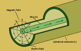
Cross section and field distribution in a coaxial cable.
In a communication system as well as being a connecting medium, a coaxial cable is an alternative for protecting data from noise. A coaxial cable consists of a central conducting wire separated from an outer conducting cylinder by an insulator. The central conductor is positive with respect to the outer conductor and carries a current . Coaxial cables do not produce external electric and magnetic fields and are not affected by them. This makes them ideally suited, although more expensive, for transmitting signals.
The factors which will influence the choice of a cable medium are:
The impedance of the cable.
Impedance is the opposition to the flow of an alternating current through the cable. It depends on several factors:-
the resistance of the metal conductors used to make the cable,
the capacitance between the two conductors,
the inductance of the wires,
the frequency of the signal being transmitted.
The impedance of a cable is important since it is necessary to "match" the impedance of the cable to the transmitter and receiver in order to minimise energy loss.
 Large
open wire feeder
Large
open wire feeder
Due to the distribution of the electric and magnetic field an open
wire feeder is not secure and does pick up noise. Samples of twisted
pairs

Inductive linkage with adjacent cables.
In telephone cable communication systems many hundreds of pairs of wires are bundled tightly together. This leads to the current in one pair inducing a current in an adjacent pair. This produces an effect called crosstalk, i.e. unwanted signals being transferred to other circuits. Crosstalk is a form of noise and is obviously undesirable. When many conducting pairs of wires are bundled together to form large cables, the pairs are twisted to reduce the overall magnetic field produced by each pair. For high speed digital communication systems, e.g. computer networks, Twisted Pair cables offer many advantages, being cheaper, smaller and having a greater bandwidth than Coaxial cable.
The signal passed along the twisted pair cable are differential, i.e. when the one wire is positive the other is negative and vice versa. On transmission, the magnetic and electric fields produced by one wire therefore cancels out the magnetic and electric fields produced by the other wire, so minimising any radiated signal. On reception, the receiver is only sensitive to differences in the signals carried by each wire, noise or other interference induced in both wires being cancelled out.
Whenever travelling waves encounter a discontinuity in the medium in which they are moving, some energy will be reflected back at the discontinuity. This is observed whenever you look through a window. Reflections occur at both glass/air interfaces. Such reflections reduce the transmitted energy along the medium and are therefore undesirable.
Care must be taken to ensure that when cables are connected or terminated, their impedances are matched to prevent this unnecessary loss of transmitted power.
Optical fibres
Optical fibres are discussed more fully in a later section, but as an introduction it is worth considering the propagation of light along optical fibres. The basic construction and principle of fibre optic systems is shown in the diagram below.
The simplest type of optical fibre consists of a fine glass fibre with a core of refractive index n2, and a cladding of refractive index n1.
n2 is greater than n1 and the ratio n1 to n2 determines the critical angle for the boundary between the core and the cladding. The core and cladding have further coatings to protect the glass from oxidation and mechanical damage.
Rays such as a and b in the diagram, which strike the core/cladding interface at an angle greater than the critical angle, are totally internally reflected whereas rays such as c which make an angle less than the critical angle with the cladding are not totally reflected. The fibre is effectively a wave guide for light rays and light injected into one end will emerge at the other even if the fibre has modest bends in it.
Noise, Distortion and Crosstalk
Noise, distortion and crosstalk are three unwanted effects in telecommunication systems. Distortion is the alteration of the signal waveform as a result of signal processing and two examples are shown in the diagram below.
In the first diagram a triangular waveform has been distorted by an amplifier being overloaded and saturating.
The second diagram shows a rectangular pulse which has been distorted by the signal processor having a poor high frequency response.
Distortion of a signal introduces frequencies into the signal spectrum that were not in the original. This often has the effect of making the signal bandwidth larger which is undesirable when signals are close together in a frequency multiplexed system.
Noise is the addition of (random) unwanted electrical energy to the required signal; an example is shown below.
Noise is unfortunately added to the signal at every point in the overall communication system. The aim is to keep the added noise to a minimum.
Channel noise is added to the signal as it passes through the transmission medium or channel. There are several sources of channel noise including:-
crosstalk as a result of capacitive and inductive linkage between adjacent conductors;
cosmic or galactic noise resulting from very energetic nuclear processes in star systems;
fluctuation noise from natural causes like electrical storms or man-made sources,
e.g. electric motors and ignition systems.
Noise is also added to the signal by the transducers and components in the signal processing system. Resistors produce Thermal or Johnson noise; this increases with temperature.
Active devices such as transistors and integrated circuits produce Shot noise as a result of electrons passing through the semiconductor junctions.
Some transmission media are immune from some types of noise; for example, crosstalk and other induced effects are not a problem with fibre optic systems.
Signal to noise ratio
The signal to noise ratio of a system could be expressed as a large meaningless fraction or as log
Signal power/noise power (Bels) but is far more usually expressed in decibels (dB) to give a finer, more accurate representation and is defined by the following equation for SNR:
If the signal to noise ratio falls below a certain level then the information in the signal will be degraded unacceptably. The minimum signal to noise ratios for various communication systems are as follows:
Land based private mobile telephone systems require at least 10 dB.
Ship-to-shore radio telephones require 20 dB.
Public service telephone systems require 40 dB.
Analogue television systems require 50 dB.
A good hifi system would typically have a SNR of 60dB
This means there would be 1 microwatt of noise power for every 1 watt of audio signal power.
Both DAB and DTT use error correction systems which can be used to reduce the effects of a poor signal to noise ratio.
Radio communication – General Principles
Student aims
:
describe the transfer of data by different types of carriers and media;
explain the need for a carrier wave;
explain how the signal amplitude and frequency are encoded on the carrier using amplitude modulation (AM);
draw time waveforms to illustrate the nature of AM including the effect of depth of modulation on the envelope;
draw
and label a frequency spectrum for a sinusoidal carrier wave
amplitude modulated by:
a single frequency signal, showing the
carrier and side frequencies
a signal consisting of a range of
frequencies, showing the carrier and sidebands;
explain and calculate the bandwidth requirements of AM signals;
explain how a signal’s amplitude and frequency are encoded on the carrier using frequency modulation (FM);
draw time waveforms to illustrate the nature of FM;
describe and calculate the practical bandwidth requirements of FM signals;
know that radio stations broadcasting in LF and MF bands use AM;
describe channel allocation within LF and MF broadcasting;
know that FM is used for entertainment broadcasting in the 88 MHz – 108 MHz VHF band;
understand and explain the relationship between channel spacing and signal bandwidth;
know that DAB broadcasting is used in the 217.5 MHz – 230 MHz VHF band, and that channels are grouped in multiplexes on different frequencies;
explain why different DAB channels are transmitted at different data rates, depending on the programme content.
A Basic Radio System
The transmission of radio waves at audio frequencies or so called baseband (20Hz - 20kHz) is possible but very inefficient; a large power output is required from the transmitting aerial to achieve even a modest range. It would also lead to there being very few possible radio stations, since they would interfere with each other. It is believed, however, that there are military systems
which have achieved a similar fete to this by using the ionosphere as a giant antenna, see HAARP.
For mere everyday would be broadcasters, this difficulty is overcome by using a much higher frequency carrier wave and combining the information signal with it. This combination of information signal and carrier signal is called modulation.
A basic radio system consists of a transmitter and a receiver. The principal elements of a radio transmitter are shown in the diagram below
The information to be transmitted (shown as the audio signal input) is amplified and then applied to the modulator along with the output from the radio frequency oscillator. These two signals are combined; they are not simply added but are effectively multiplied or ‘mixed’ together resulting in the generation of extra frequencies or so-called sidebands. . The modulated radio frequency signal is then power amplified to provide an effective power level for sending to the aerial.
This basic transmitter system is applicable to any of the various modes of modulation.
The basic block diagram of a basic radio receiver is shown in the diagram below.
The aerial receives radio waves from transmitting stations, and other sources of electromagnetic waves, which induce alternating currents in the aerial. The desired frequency range is then selected by the tuned circuit(s). These alternating currents are often very small and may be amplified before the demodulation stage. The demodulator removes the radio frequency carrier component and restores the original audio signal. The audio signal is then amplified to give a suitable output from a loudspeaker or earphones.
There are several modulation processes the most common being:-
amplitude modulation, AM,
frequency modulation, FM,
pulse code modulation, PCM,
frequency shift keying, FSK,
quadrature phase shift keying, QPSK and
quadrature amplitude modulation, QAM
Amplitude Modulation
Amplitude modulation is used by commercial radio broadcasters in the long, medium and short wave bands.
The diagram below represents an Amplitude Modulated wave. In amplitude modulation, the magnitude of the carrier is varied in accordance with the amplitude of the information signal.
With an amplitude modulated wave the amplitude of the radio frequency carrier is varied in proportion to the audio frequency or information signal, as in the diagram above. The amount, or depth, of modulation depends upon the ratio of the amplitude of the information signal to the amplitude of the carrier wave signal.
Depth of modulation
Consider the diagram below: x is the modulating signal amplitude and y is the carrier wave amplitude.
The modulation depth, m, of the resulting amplitude modulated signal is defined by:
The modulation depth of the waveform in the diagram below is approximately 65% and can be verified by measuring the amplitudes of the waves in the diagram. The peak amplitude of the modulated wave is the sum of the modulating and carrier waves. If x is equal to y then the carrier is 100% modulated. If x is increased further then over modulation occurs and the region represented by y-x in the diagram becomes zero.
When the depth of modulation exceeds 100%, the information will be distorted and the bandwidth of the signal will be increased as a result of the carrier actually disappearing. However, if the modulation depth is too small then the received signal will be of poor quality because the signal-to-noise ratio will be reduced. The usual depth of modulation for good quality reception is approximately 80%.
Diagram (a) below show an amplitude modulated wave at 100% and diagram (b) shows an amplitude modulated wave that is being over- modulated (i.e. greater than 100%). Both diagrams assume the same carrier amplitude as for the diagram above.
Over-modulation or greater than 100% modulation is very undesirable as it leads to transmitted distortion and excessive bandwidth which will interfere with adjacent frequency broadcast stations.
Side Frequencies
The process of modulation results in the production of frequencies other than those of the carrier and the modulating signal. When a modulating signal or information frequency fi, is combined with a carrier wave of frequency fc, then a signal comprising of three frequencies, (fcfi), fc and (fc+fi), results as shown in the diagram below.
amplitude
carrier frequency
fc – fi fc fc + fi
For all but modulated with a pure sine wave or single audio tone, the modulating signal will usually consist of a band of frequencies, the resulting frequency spectrum of the modulated signal will be as shown in the diagram below.
If the frequency of the modulating signal ranges from 100Hz to 4.5 kHz then the lower sideband will range from (fc4500)Hz to (fc100)Hz, the upper sideband will range from (fc+100)Hz to (fc+4500)Hz, and the bandwidth of the transmitted radio signal will be 9 kHz or twice the bandwidth of the modulating signal. 4.5 KHz is the normal maximum modulating frequency allowed in long and medium wave broadcasting and channel separation is thus 9 KHz for obvious reasons.
For example, BBC Radio 5 is on 693 kHz and 909 kHz.
6 + 9 + 3 = 18, 9 + 0 + 9 = 18,
1 + 8 = 9. 1 + 8 = 9.
Virgin Radio is on 1215 kHz and 1242 kHz.
1 + 2 + 1 + 5 = 9. 1 + 2 + 4 + 2 = 9.
Check your local stations on the medium wave.
It is possible to suppress one of the sidebands and the carrier if there is a constraint on channel bandwidth. Since it is only the information in one sideband that is needed on reception, the power that would put into transmitting the carrier and the other sideband, in a normal AM signal, can be concentrated into just the one sideband, resulting in a much more potent signal. Such methods are used in marine, some military and in amateur radio transmission.
In an FM system, the amplitude of the information signal controls the frequency of the carrier wave. The frequency of the information signal controls the rate of change of the carrier frequency. This is easier to see in a diagram:
Time waveforms to show the nature of FM
Each graph shows the variation of voltage against time.
The first graph shows the high frequency carrier signal, the second the low frequency information signal and the third the effect of frequency modulation of the carrier by the information signal.
It can be seen that as the information signal increases and becomes positive, the frequency of the carrier increases and as the information signal decreases and becomes negative, the carrier frequency is reduced.
FM is used in high quality radio transmission and a typical FM carrier frequency (for radio transmission) is between 88-108 MHz and the maximum frequency deviation is limited, by international agreement, to 75kHz.
The bandwidth of an FM signal is, theoretically, very broad, but in practice the outer extremities of the frequency spectrum of an FM signal can be omitted without causing audible distortion.
It is not possible to draw a frequency spectrum for an FM signal because the sidebands produced are more complex, but the practical bandwidth can be calculated by adding the highest information frequency to the maximum deviation and doubling the result.
Bandwidth = 2 x (maximum deviation + max. information freq.)
Since on the VHF FM band, since the deviation is ±75 kHz and the highest information frequency is 15 kHz, the bandwidth of the modulated signal is:
2 x (75 + 15) = 180 kHz
Since stereo information is also carried, the channels are actually made to be 200 kHz wide, but the carrier frequencies are spaced every 100 kHz due to the short-range nature of VHF radio signals. Frequencies can then also be re-used at distance, very similar to the situation with mobile telephones, see section 6.
Frequency modulation also produces sidebands and the bandwidth of an FM signal is approximately given by 2(f + fm) where f is the maximum deviation and fm is the highest modulating frequency. There has to be a compromise between the improved quality that accompanies increased bandwidth and the restriction of the number of channels available in a frequency band.
Advantages and disadvantages of AM and FM transmissions.
AM and FM are both used for radio transmission. AM is used for low cost transmitters and receivers because the circuitry used is simpler in comparison with that used in FM.
AM transmissions are, however, more susceptible to noise and distortion. Any electric spark, e.g. from a motor, a switch etc., will produce electromagnetic waves with a wide range of frequencies (impulsive noise) which will interfere with amplitude modulated signals. Such interference shows itself as loud crackles on a radio and therefore, adversely affects the quality of AM signals. Impulsive noise is random in nature and difficult to eliminate in the receiver.
AM signals also suffer from fading. Fading is the result of differences in phase between waves travelling via paths of different lengths through the ionosphere or as a result of reflection from large dense objects like steel reinforced buildings or vehicles. The strength of the signal at the receiver will be the sum of all of the waves and may be larger or smaller than one wave on its own, since the phases may be such as to aid or oppose. Since the paths usually change with time, the result is variations in the received signal strength, or fading. Fading is most noticeable on the medium and short wave bands in the early evening as waves start to be received after reflection by the ionosphere.
It frequently happens that the propagation conditions are different for waves of slightly different frequency. So in the case of voice or music modulated signals, the carrier and different parts of the sidebands will have different amplitude and phase shifts resulting in severe distortion. This is known as selective fading.
A principle advantage of FM transmission over AM is its improved immunity to impulsive noise. Impulsive noise produces momentary variations in the amplitude of the signal which are suppressed in an FM receiver by a limiter circuit. The limiter circuit is simply an amplifier in saturation so the output is not capable of rising as a result of impulsive noise. FM transmission is used for high quality signal transmission, but at the cost of a much wider bandwidth and a more complex receiver. Most commercial FM stations use the VHF waveband since it enables the larger bandwidth to be accommodated, but such high frequencies can make circuit design more difficult.
As a result of FM stations using the VHF band, such transmissions are of limited range (line of sight) because the ionosphere does not reflect VHF waves. It should be noted, however, that this is not a limitation of frequency modulation but of the waveband that is used. This means that more transmitters are needed for nation-wide coverage, although it does permit stations which are geographically separate (> 200 kilometres) to operate on adjacent parts of the band without causing interference. This makes VHF FM useful for local radio stations.
Broadcast stations
The lowest frequency used in the broadcast long wave radio band is 153kHz and extends up to a frequency of 281kHz. Radio stations are distributed through out this frequency range and are spaced every 9kHz. The most obvious long wave band radio station in the UK is Radio 4 which is transmitted on a frequency of 198kHz.
The lowest frequency of the medium wave band is 520kHz and extends up to a frequency of 1611kHz. Radio stations are spread throughout this frequency range and are spaced every 10kHz in North and South America and Canada and every 9kHz for the rest of the world.
On the broadcast short wave bands, between 2.3MHz and 26.1MHz, the radio stations are spaced every 5kHz, although there are some frequencies in the above range that are allocated to other services, including Amateur Radio.
The 9 (10)kHz spacing of the LF and MF radio stations severely limits the bandwidth of the information that can be modulated onto the carrier wave. Taking into account the upper and lower sideband, the bandwidth of the information is limited to about 4kHz.
The broadcast VHF FM radio band begins at 88.6MHz and extends to 104.6MHz. The radio stations are spaced every 200kHz. The much larger channel spacing on the VHF band allows the use of FM and a corresponding increase in the bandwidth of the information modulated onto the carrier. However, these radio stations usually transmit stereo broadcasts and much of the bandwidth is used to facilitate this. The bandwidth of the left and right hand information channels is limited to 15kHz (a significant improvement on the 4kHz of the medium wave transmissions). The left and right hand channels are then added together and the information is used to frequency modulate the carrier. However, the left and right hand channels are also subtracted from each other as well, and this information is amplitude modulated onto a separate sub carrier at 38kHz. This signal is also used to frequency modulate the main carrier.
The maximum bandwidth of the FM broadcast transmission is limited to 150kHz, so ensuring that each transmission is accommodated within the 200kHz channel spacing.
Analogue broadcast television stations transmit in the UHF band which starts at 471.25MHz, with the designation of channel 21, and extends to 847.25MHz, with the designation of channel 68. The television channels are evenly distributed into this frequency range and have a channel spacing of 8MHz.
Digital Audio Broadcasting (DAB)
The DAB system was designed in the late 1980s, and its main original objectives were to:-
provide radio at CD-quality,
provide better in-car reception quality than on FM,
use the spectrum more efficiently,
allow tuning by the name of the station rather than by frequency and
allow data to be transmitted.
DAB Digital Radio is based on the European Eureka 147 specification and is now a world standard. It is currently available to over 300 million people in almost 40 countries, with over 600 different services, and these numbers are increasing daily. Transmissions are in the 217.5 to 230MHz sub-band of VHF Band III (170–230MHz); and 1452 to 1492MHz, at the upper end of the UHF L-Band (500–1500 MHz).
DAB works by combining two digital technologies to produce an efficient and reliable radio broadcast system.
Firstly, MUSICAM (a version of MPEG2), is a compression system, that reduces the vast amount of digital information required to be broadcast. It does this by discarding sounds that will not be perceived by the listener - for example, very quiet sounds that are masked by other, louder sounds - and hence not required to be broadcast, and efficiently packages together the remaining information.
The second technology, COFDM (Coded Orthogonal Frequency Division Multiplex) ensures that signals are received reliably and robustly, even in environments normally prone to interference. Using a precise mathematical relationship, the MUSICAM signal is split across 1,536 different carrier frequencies, and also across time. This process ensures that even if some of the carrier frequencies are affected by interference, or the signal disturbed for a short period of time, the receiver is still able to recover the original sound.
The interference which disturbs FM reception, caused by radio signals "bouncing" off buildings and hills (multipath) is eliminated by COFDM technology. It also means that the same frequency can be used across the entire country, so no re-tuning of sets is necessary when travelling, or taking a portable receiver to a different area.
Broadcasts are made from transmitters providing groups of stations on a single frequency, known as multiplexes or ‘ensembles’, and in a given area, several different ensembles may be able to be received.
The frequencies allocated to the multiplexes are allocated a code number and a centre frequency. Those available, at the time of writing, in the UK are given in Appendix D.
A DAB multiplex is made up of 2,300,000 "bits" which are used for carrying audio, data and an in-built protection system against transmission errors. Of these about 1,200,000 bits are used for the audio and data services. Throughout the day a different number of bits may be allocated to each service.
There are currently three National multiplexes, one run by the BBC and the other two by commercial operators. Each of the national multiplexes operates as a Single Frequency Network (SFN). This means that all the BBC transmitters for their national multiplex use exactly the same channel, and transmit the same modulation pattern and carrier frequencies in a synchronised manner. If this were attempted using conventional analogue modulation systems the result would be that the transmissions would interfere with one another and reception would be impossible in many places around the country. However, a time delay (guard interval) of 246µs is used between the transmitters and so the signal from more than one of the transmitters can be used by the receiver. This is quite a useful feature of DAB as it saves having to allocate different frequencies for the same stations in adjacent areas to avoid interference.
The DAB channel allocated to the BBC for its ‘national’ sound radio broadcasts is centred on 225·64 MHz. This multiplex currently carries all the main BBC sound radio stations – Radio 1, 2, 3, 4, etc. The nominal width of the channel is 1·75MHz and the system uses 1536 sub carriers, each spaced 1kHz apart, which occupies 1.536MHz of the channel. This leaves around 100 kHz either side for the modulation sidebands, and to make it easier for RF/IF filters in a receiver to accept a wanted transmission whilst rejecting others in adjacent channels.
Each sound radio station first produces the audio in the form of Linear Pulse Code Modulation (LPCM) with a sampling rate of 48,000 samples/sec, with 16 bits per sample. This means that the initial bit rate for such a stream of stereo audio will be48000 × 16 ×2 = 1·536 million bits per second. For various reasons, the useful data rate for a DAB multiplex is only around 1·2 Mb/s. which is not quite enough to carry the LPCM for a single audio station!
In order to reduce the bit rates required for audio, the broadcasters use MUSICAM to give an output having a bit rate much less than 1·2Mb/s. The MUSICAM system can provide various rates from 384 kb/s down to 32 kb/s, with the audible quality of the results falling with the chosen output bit rate. At a bit rate of 256kb/s per stereo audio stream we could expect to fit four or five sound radio stations onto a single DAB multiplex. However, in the UK at present, quantity seems to count for more than quality and so most of the music stations use 128kb/s. This means that around ten stations can be fitted onto a multiplex, but the level of data reduction is such that audible effects may become noticeable, albeit not objectionable to listeners who have no interest in ‘hi-fi’. For mono voice transmissions, the bit rate can be reduced to as low as 32kb/s.
The MUSICAM encoded data for the stations on a given multiplex is first arranged into ‘Logical Frames’ which represent sections of the audio signal which are 24 ms long. These are also called a Common Interleaved Frame (CIF). Four CIFs are grouped together to make up a Transmission Frame (TF).
Each of the CIFs assumes that the data rate is 256kb/s. However, most transmissions are only at 192kb/s or lower, so freeing up space for the FIC and other broadcast transmissions.
Digital information is transmitted as ‘symbols’, and for COFDM, each symbol represents 2 bits of information.
For various reasons, most of the transmission frames are interleaved apart from the Fast Information Channel (FIC). This FIC contains data that is not time-interleaved, so can be read immediately by the receiver. The FIC provides information on topics like which of the following symbols relate to which stations, and what stations are being broadcast, etc. This then allows the receiver to pick up and decode only the data from the rest of the frame which relates to the station which the user has chosen to hear. The FIC also allows the tuner to detect when the details of the multiplex alter – e.g. when a ‘new’ station starts broadcasting, or the one being listened to changes its bit rate in response to some other station starting or finishing for the day. Thus the system is designed to be flexible, and allow the receiver to adapt to changes in the transmissions as they occur.
Although grouped into 96 ms frames for transmission purposes, the actual audio data is interleaved and spread over more than one frame. In practice, UK DAB interleaves audio data over a range of 360 ms. This means that even when some audio data is completely lost and can’t be recovered, the result should be a slight inaccuracy spread over more than a quarter second rather than simply a ‘click’ or momentary silence. The drawback of this extended interleaving is that the receiver has to wait this long for all the relevant information to arrive before it can reconstruct the sounds. Hence it adds an extra delay into the communication process. In practice, however, there will already be delays due to the time needed to MUSICAM encode/decode, etc. so delays of the order of 1·5 seconds during the entire transmission and reception process are fairly normal. These delays may also vary from station to station, and with the design of the receiver being used.
DAB Summary Exam Requirement
Digital Audio Broadcasting DAB
A recent development is digital audio broadcasting (DAB). This has been introduced across most of the UK on a different VHF band, from 217.5 MHz – 230 MHz Due to its digital nature, the reception is practically perfect and could supersede FM in the future. Groups of stations are multiplexed together on channels spaced at 1.712 MHz intervals, for instance all BBC stations tend to be transmitted together. Stations are categorised into different bandwidth requirements and transmitted at different bit rates, BBC radio 3 (classical music in stereo) is transmitted at 192kbps whereas stations that carry traffic news are transmitted in mono at 48kbps.
|
BROADCASTING BANDS SUMMARY |
|
|
|
||
|
|
|
|
|
||
|
Band |
Frequencies |
Wavelengths |
Modulation |
||
|
|
|
|
|
||
|
LW |
100-300 KHz |
3000-1000m |
AM |
||
|
MW |
500-1500KHz |
600-200m |
AM |
||
|
SW |
3-30 MHz |
100-10m |
AM |
||
|
VHF |
30-300 MHz |
10-1m |
FM |
||
|
|
|
|
DAB |
||
|
UHF |
300-1000MHz |
1m-30cm |
DVB |
||
|
|
|
|
GSM |
||
|
Microwaves |
>1000MHz |
<30cm |
G3/G4 |
||
|
|
|
|
Wifi |
||
Theory Questions
1. The highest frequency in the short wave band is
2. In an AM system, a carrier wave of 10V rms is modulated
by an information signal of 8V rms.
Calculate the depth of modulation produced.
A 504 kHz carrier wave is modulated by a 3 kHz information signal.
3. What is the upper side frequency?
4. What is the lower side frequency?
5. The 3 kHz information signal is replaced by a band of
frequencies from 100 Hz to 4.5 kHz.
What is the total bandwidth of the modulated wave?
6. At what intervals are all MW radio channels are spaced?
7. An FM signal has a deviation of ± 10 kHz and a highest
information frequency of 3 kHz. Calculate the bandwidth of
the resulting modulated signal.
8. A radio wave has a frequency of 30 MHz.
Calculate the length of a half-wave dipole for this frequency.
9. The Channel spacing for DAB channels is
10. The data rate for Radio 3 on DAB is
Radio receivers
Student Aims
describe and explain the function of the systems within a simple radio receiver, consisting of an aerial, tuned circuit, detector/demodulator and earphone;
calculate the optimum length for a half-wave dipole for a given wavelength/frequency;
know that the impedance of the antenna should match that of the feed;
describe in qualitative terms, how voltage and current vary in a parallel LC circuit near resonance;
know that resonance occurs when XL = XC and hence calculate the resonant frequency;
draw a resonance curve for a parallel LC circuit;
explain the use of a LC network to select a particular frequency;
explain the significance of the quality factor of a tuned circuit and its relationship to the selectivity of the receiver;
use the
resonant frequency formula to calculate suitable values of L
and C
;
explain how an rf amplifier can be used to improve sensitivity;
draw a block diagram for a superhet receiver consisting of an aerial, rf amplifier, local oscillator, mixer, if amplifier and filter, demodulator, AGC, af amplifier and loudspeaker;
describe the principle of operation of the superhet;
describe the frequency spectrum at the output of the mixer, limited to the main mixer products of the two input frequencies and the sum and difference frequencies;
describe the advantages and disadvantages of the superhet receiver over a simple receiver
A little history
The first radio receivers were crystal sets, and became available in the 1920's with the opening of Marconi's first broadcast station in Chelmsford.
A crystal set does not have a battery. It runs completely from the energy extracted from radio waves it picks up from the antenna. A resonant LC (or tuned) circuit coupled to a large aerial or antenna was used. Many amateur experimenters constructed crystal sets, often with the tuner inductor coil wound on a tubular box or a drinking glass. At this time the semiconductor diode had not been invented, so extracting the audible modulation signal from the transmission relied on the non-linear electrical properties of the 'crystal', typically a piece of coke or galena. In early sets a "cat’s whiskers" - a fine piece of wire - was adjusted by trial and error to make a suitable contact with the crystal.
There were many limitations to the crystal set: it needed a big aerial (antenna), an earth connection, the clumsy cat’s whisker, and the weak signal could only be listened to by one person at a time with headphones. Very quickly the crystal set began to be replaced by valve radios with loudspeakers, powered by batteries.
In World War II, crystal sets were used by prisoners of war in prison camps to listen to news from home. Much ingenuity went into improvising the necessary components.
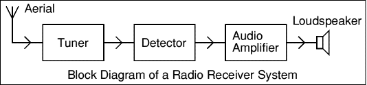
The power supply (not shown) is connected to the audio amplifier block.
Aerial - picks up radio signals from many stations.
Tuner - selects the signal from just one radio station.
Detector - extracts the audio signal carried by the radio signal.
Audio Amplifier - increases the strength (power) of the audio
signal.
This could be broken down into the blocks like the Audio
Amplifier System shown above.
Loudspeaker - a transducer which converts the audio signal to sound.
Simple Crystal Radio
The crystal radio gets its name from the galena crystal (lead sulfide) used to rectify the signals. A "cat's whisker" wire contact was moved about the surface of the crystal until a diode junction was formed. The 1N34A germanium diode is the modern substitute for galena and most other germanium small-signal diodes will also work well. Silicon diodes are not a good choice because their much higher barrier potential requires larger signals for efficient rectification. Certain silicon Schottky diodes with low barrier potential will work well but most small-signal Schottky diodes will not perform as well as a garden-variety germanium diode.
|
|
The circuit is quite simple but many pitfalls await the novice. The first precaution is most important! The crystal radio works best with a long, high outdoor antenna but the beginner may not fully appreciate the danger of bringing such a wire into the house. Lightning strikes to the antenna will probably destroy the crystal radio but if precautions are not taken, much more damage will result. The best strategy is to incorporate a commercial lightning arrestor with a straight, heavy gauge ground wire leading down to a buried water pipe. It is not sufficient to disconnect the antenna from the receiver during thunderstorms.
Other pitfalls are less dangerous and relate to the receiver's performance. A common mistake when building a crystal radio is to load the tuned circuit excessively. The Q of the tuned circuit must remain high to give selectivity or strong radio stations will all mix together. A good design will usually have low-impedance taps on the inductor for connections to the antenna and diode as shown in the schematic. A long wire antenna with a good ground connection will connect to the lowest impedance tap whereas a shorter antenna with no ground connection may connect to a higher tap. The diode may be experimentally moved to different taps and even across the whole coil for maximum sensitivity. The antenna and diode connection may be made with alligator clips for easy experimentation.
|
|
Another potential problem area is the earphone. Not all crystal earphones are sensitive and the experimenter should test a few to get a "good" one. High impedance dynamic earphones are a bit more reliable and can give excellent results. Try an old telephone receiver or a modern portable tape player headset (some are high-Z and fairly sensitive). Low impedance earphones like those used with many portable radios will not work at all. A simple test is to hold one earphone wire between the fingers while scraping the other lead across a large metal object like a file cabinet. If static is heard in the earphone it will probably work well with the crystal radio.
The variable capacitor is often connected incorrectly. Make sure to connect the rotor to ground and the stator to the "hot" side of the coil. Otherwise, the radio will detune when the capacitor knob is touched. If detuning is noticed then try reversing the connections.
Some experimenters are tempted to omit the 82k resistor which discharges the capacitor on the theory that it wastes precious signal power. With a typical germanium diode, this little "improvement" may work somewhat but only because the diode has significant leakage and the performance will not be predictable. A dynamic earphone may be DC coupled eliminating the need for the resistor.
The coil may be wound on a 1.5 inch PVC pipe coupler as shown in the drawing. These typically have an outer diameter of about 2.2". Drill two small holes at each end to secure the ends of the coil. The wire type is not particularly critical but select a gauge and insulation so that the 65 turns cover about 2/3 of the coupler. An excellent choice is 30 AWG "wrap" wire from Radio Shack. The prototype uses this solid conductor wire with blue insulation. This wirewrap wire is available in 50' lengths on little spools and about 37' will be needed. A "loopstick" coil may be used in place of the coil shown. These coils have an adjustable ferrite core for tuning so a fixed value capacitor may be used in place of the variable capacitor shown. The coil, capacitor and a terminal strip for the other parts may be mounted to a small wooden board. (See photo of receiver with transistor amplifier below.)
|
|
If a metal chassis is used then the coil must be mounted horizontally and above the metal to prevent unacceptable loading.
Here are some alternative construction ideas:
Fahnestock clips make excellent connectors for the antenna and ground wires. The coil may be mounted above the board or chassis with angle brackets by adding another bend, as shown below. The windings may be quickly secured with a single layer of colored "Duck" tape that is now available in more attractive colors than gray or black. The taps to the coil can be located at the rear, near the bottom so that the unavoidable bulges in the tape don't show. An ordinary piece of wood may be quickly finished by applying adhesive-backed PVC film intended for kitchen cabinets. Just stick it on and trim flush with scissors.
TRF Receivers
The simple radio or crystal set lacked both sensitivity ( the ability to pick up weak stations) and selectivity(the ability to separate one received station from another) for this reason TRF was developed. Early valve radio receivers were of the Tuned Radio Frequency (TRF) type consisting of one or a number of tuned radio frequency stages with individual tuned circuits which provided the selectivity to separate one received signal from the others. A typical receiver copied from a 1929 issue of "The Listener In" is shown in Figure 1. Tuned circuits are separated by the radio frequency (RF) amplifier stages and the last tuned circuit feeds the AM detector stage. This receiver belongs to an era before the introduction of the screen grid valve and it is interesting to observe the grid-plate capacity neutralisation applied to the triode RF amplifiers to maintain amplifier stability. In these early receivers, the individual tuning capacitors were attached to separate tuning dials, and each of these dials had to be reset or tracked each time a different station was selected. Designs evolved for receivers with only one tuning dial, achieved by various methods of mechanical ganging the tuning capacitors, including the ganged multiple tuning capacitor with a common rotor shaft as used today. Even then because coils could not be perfectly matched tracking trimmer capacitors had to be used. Tracking is very difficult to achieve even with these refinements and in practice the number of tuned circuits that can be adjusted together is limited to a maximum of three. Another problem with TRF was that the selectivity was good when receiving low frequencies but not so good at higher frequencies and thus the TRF radios had an unavoidable ‘variable’ selectivity factor!
A solution to this problem was found by Edwin Armstrong in 1918 in the form of the “Supersonic Hetrodyne Receiver” often shortened to ‘superheterodyne ’ and nowadays just called ‘superhet’.
The superhet receiver overcomes this problem by changing the frequency of the required radio station to an intermediate frequency. In long and medium wave radios this intermediate frequency is 455kHz. A VHF FM receiver would use an intermediate frequency of 10.7MHz while a television receiver uses an intermediate frequency of 39.5MHz.
The diagram below shows the block diagram of a superheterodyne (superhet) radio receiver.
The rf tuner provides improved sensitivity and some selectivity and is tuned to the desired station.
This signal is then mixed with a higher frequency signal produced by the local oscillator.
e.g. If the required station had a carrier frequency of 1.00MHz, then the local oscillator would produce a signal of frequency 1.455MHz. These two signals are then mixed together resulting in signals of frequency 2.455MHz (the sum) and 0.455MHz (the difference), as well as the two original signals (1.00MHz and 1.455MHz). All four signals are passed into the intermediate frequency (if) amplifier.
The if amplifier contains many (>6) tuned circuits, all adjusted to the intermediate frequency. It therefore has a well defined bandwidth and provides the extra selectivity needed to eliminate radio stations on adjacent frequencies. All of the signals from the mixer will be rejected except for those around the intermediate frequency, (i.e. 455kHz).
Tuning of a superhet receiver is by simultaneously adjusting the resonant frequency of the rf tuner and the frequency of the local oscillator. This is often achieved by using a dual gang variable capacitor, one part for the rf tuner and the other for the local oscillator.
After the radio signals have been converted to the intermediate frequency and amplified they are then demodulated. For an AM signal this is achieved by a diode as in the simple receiver. The demodulated signal can then be filtered and amplified to operate a loudspeaker.
The automatic gain control, (AGC), automatically adjust the gain of the if amplifier to accommodate changes in signal strength from the radio stations. It is also to minimise the effects of fading.
The advantages of the superheterodyne receiver over the simple receiver are:-
improved selectivity, because of the multiple tuned circuits at the intermediate frequency
improved sensitivity, because of the if amplifier.
The disadvantages of the superhet receiver are:-
at high frequencies the local oscillator can drift in frequency, although with modern designs this can be reduced or even eliminated,
image response interference.
Consider the example above where a 1.00MHz signal is being received on a radio with an if of 455kHz. The local oscillator has a frequency of 1.455MHz and so, when mixed with the 1.00MHz signal, a signal of 455kHz is produced. But if a radio signal at a frequency of 1.91MHz was also present it would also be mixed with the local oscillator to give a frequency of 455kHz (1.91MHz - 1.455MHz = 0.455MHz). If the radio station on 1.91MHz was not attenuated sufficiently by the rf tuner then it would cause interference.
The rejection of image signals is also a reason that a higher intermediate frequency is used for the VHF band compared to the medium wave band.
An interesting variation of the superhet receiver is the direct conversion receiver. This is essentially a superhet receiver but with an intermediate frequency of 0Hz. The local oscillator is on the same frequency as the required radio signal and so, when mixed together, an audio signal corresponding to the radio signal's sidebands is produced. This audio signal can then be amplified with high gain, low noise audio amplifiers to provide a loudspeaker output.
Such receivers, though much simpler to build, do not produce such high quality audio. It is also essential to ensure that the local oscillator is on exactly the same frequency as the carrier otherwise a loud objectionable oscillation is heard at the beat frequency.
The block diagram of a FM superhet receiver is shown in below. It is very similar to the AM version but with the following differences.
There is automatic frequency control (AFC) to stabilise the local oscillator frequency against drift.
The if amplifier needs a wider bandwidth than an AM receiver and this is achieved by staggering the resonant frequency of the tuned circuits.
The last stage of the if amplifier is arranged so that it is saturated by the received signal and is known as a limiter. This is necessary so that the demodulator does not detect any amplitude variations in the signal.
The demodulator required for FM is rather more complicated than the single diode used for AM.
There are several methods of extracting the af signal from the FM carrier. The older demodulators, including the 'frequency discriminator' and the 'ratio detector', are beyond the scope of this specification and are not required.
Slope detection uses a tuned circuit resonating slightly above or below the carrier frequency, as shown below. As the frequency varies with the af modulation, the amplitude of the signal developed across the tuned circuit will vary, so producing an AM signal which can be demodulated in the normal way.
Pulse counting detection relies on the output signal from the if amplifier consisting of positive going pulses that are all the same amplitude, but varying in width with the modulation. If these pulses are averaged over a number of cycles of the intermediate frequency then an output will result that is proportional to the modulation, i.e. the information signal.
The introduction of integrated circuits containing fully functional phase locked loops has led to a modern and very popular method of demodulating FM, but an full explanation of these is beyond the scope of this publication and not .
An analogue signal is one that can vary to take any value between set limits. The voltage waveform from a microphone or to a loudspeaker is an analogue signal.
Analogue signals were first used for voice communication over wires (the telephone) and in radio systems. They suffer from the disadvantage that, as the distance over which communication increases, the signal gets weaker and noise is introduced into the system. There is no real way of removing the noise from the signal when it has been introduced, so the quality of the communication gets poorer and poorer until it is unusable.
Digital communication is now well established. A digital signal is composed of 0s and 1s given out by logic gates. A way is found of using the signal from a microphone or video camera, to control a data stream of 0s and 1s to represent the information to be communicated (audio or video). When a digital signal is communicated over a long distance, it gets weaker, but the 0s and 1s can still be recognised and separated from any noise introduced into the system. The digital signal can be recovered, cleaned up, and sent on its way by a regenerator, whereas an audio signal can only be boosted by a repeater, which will boost the noise as well as the signal.
Digital communication has other advantages also. Digital signals can be processed by logic systems, which are easy to integrate, and are very common due to the number of PCs in use. But tuned circuits used in communication cannot be integrated and so remain bulky and inconvenient.
It is easier to combine several digital signals into one data stream using a multiplexer, than it is to attempt the same process with analogue signals.
Digital signals can have more security since they are coded, and further coding or encryption can be added. Many entertainment films have shown in the past how easy it is to ‘tap’ into an analogue phone line to ‘listen in’, or more recently the use of a ‘scanner’ receiver to pick up radio signals carrying analogue audio.
Digital signals can also be compressed to save bandwidth. It is now possible to send a good quality videoconference signal comprising two-way colour video signals and two-way audio, over a 128kbps ISDN telephone link.
Digital signals are becoming more convenient as technology improves. In the space of one analogue TV channel, eight digital channels can be established, which is a much better use of bandwidth, and a better quality picture results at the receiver, since noise is removed.
There are four common techniques for converting an analogue signal into a digital signal. Since digital signals are either on or off, they can be communicated as pulses of carrier wave and so they are collectively known as pulse modulated signals.
The amplitude of each pulse carries the instantaneous amplitude of the analogue signal. This is a digital signal, but since the amplitude of each pulse is important, it is not a binary signal. There are two types of PAM, uni-polar and bipolar, in the former the information signal is offset so that the entire PAM signal is positive going. In the latter the signal can go both positive and negative. We shall only consider uni-polar PAM.
This type of signal cannot be regenerated once noise has been added to it, since the amplitude information is critical. This type of signal is often generated as a preliminary step towards producing a pulse code modulated signal.
An analogue signal can be converted into a PAM signal using a sample and hold sub-system which, triggered by a regular series of pulses, samples the amplitude of the analogue system and holds that amplitude for a set time after each pulse. The resulting series of regularly spaced pulses of varying amplitudes is the PAM signal as shown on the previous page.
Analogue PAM signal
signal
The pulse generator must produce pulses at a minimum of twice the highest frequency of the analogue signal, for the PAM signal to be able to be accurately converted back into its original form. This is the so-called Nyquist criterion.
The PAM signal can be fed into an ADC so that the amplitude of each pulse is converted into a binary number. This binary number can have any number of bits, and the more bits, the more accurately the digital output represents the analogue input. A practical system would use an 8-bit ADC operating at 8,000 samples per second. This would generate 8,000 8-bit bytes per second, which is 64 kbps of the digital telephone line.
Using an ADC always results in quantization error. If an 8-bit ADC quantizes an analogue signal of range 0 V to 2.55 V, then the output signal can represent 255 levels above 0V, making 256 levels in total , which in this case will be of 0.01 V steps, so that is the quantization error in this case.
In general, the quantization levels (and error, since 1 step is the maximum possible error) in a n-bit system having a maximum analogue input of a is
Quantization error = a ( max signal volts )
2n ( n bits)
This can also be expressed as a percentage distortion on the original signal as:
x 100% e.g 0.39% for 8 bit system
2n
This is a system where the width or time duration of a series of pulses conveys the amplitude information from the original analogue signal. PWM can be derived from a PAM signal using the amplitude of the PAM pulses to control the charge or discharge of a capacitor, causing a variable time delay before the PWM pulse goes back to logic 0. All PWM pulses are of identical amplitude; therefore this system can be used with noise reduction techniques.
To convert PWM to PPM, a short period falling edge triggered monostable may be used, see practical work.
As well as in communications, PWM is used to control motor speed in battery operated drills and screwdrivers. Squeezing the trigger controls the width of the pulses, and so the power fed to the motor. PWM is very useful in controlling DC supplies to act as a speed controller or light dimmer.
In PPM, the position in a time frame of a narrow pulse conveys the amplitude information from the original analogue signal. PPM can be easily derived from PWM by using the end of each PWM pulse to trigger production of a narrow pulse. The pulses in PPM are all of the same time duration and amplitude so this system can also be used with noise reduction techniques.
As well as in communications, PPM is often used to convey control signals to radio controlled model aircraft. The control signals generated in the controller are sent via PPM signals to the model where they control servomotors that are linked to the rudder and elevators etc.
It is essential that the sampling rate for converting an analogue signal to a digital form is at least twice the highest frequency contained in the analogue signal. In this way, the alternating positive and negative half-waves are converted to a varying PAM signal.
If the sampling rate were lower than this, information would be lost. Examine this case where the sampling rate is the same as the highest analogue frequency:
Each of the PAM pulses is the same, conveying no information about the analogue wave.
Sample rate and Resolution
The number of times per second that the voltage of a signal is measured (Sample rate) and the number of bits within each measurement (Resolution) determine the overall amount of data that must be transmitted each second, (bit rate).
E.g. The audio signal for a mobile phone is sampled 8000 times per second, and each sample generated a byte (8 bits) of data. The bit rate for the data is therefore
8 × 8000 = 64000b/s.
The bit rate is therefore 64kb/s.
E.g. An audio CD contains data that is sampled 44100 times per second and each sample is 16 bits per channel. The bit rate that must be read from the CD is
44100 × 16 ×2 = 1411200 = 1.4112Mb/s
Half and Full Duplex communication links
With any transfer of digital information between two devices it is unusual if the flow of information was only in one direction. It is more normal for information to be exchanged between the two devices. There are two distinct ways in which this can be achieved.
In the first method, only one device transmits information at a time, the other device 'listening' or receiving the information. When the transmitting device has sent its information then it becomes a receiver and listens to the information being sent to it by the other device. This mode of exchanging information is known as Half Duplex. It has the advantage that it only needs one transmission medium linking the two communicating devices, but it has the disadvantages that the transmitting device has to finish before the other device can transmit. This can slow down the transfer of information considerably in a noisy environment where it is necessary to keep retransmitting portions of the data.
The second method involves both devices being able to transmit and receive data simultaneously and is known as Full Duplex. It has the advantage that data can be exchanged much quicker, and in a noisy environment requests to repeat data can be made much quicker. The main disadvantage of Full Duplex operation is that usually two completely separate transmission channels are required.
Serial transmission
The vast majority of digital information is now transmitted Serially, i.e. one bit followed by the next etc., since much of the data is time distributed by its very nature, i.e. speech, video pictures etc.
When all the data to be transmitted is present before the start of the transmission, it could be transmitted much faster if it could be distributed to several transmitters, all transmitting the information simultaneously, i.e. parallel data transmission. The big advantage of parallel data transmission used to be its speed, but recent advances in serial communication techniques (Firewire, USB, SATA, etc) have rendered it largely obsolete.
However, when the channel bandwidth for serial communication is small, many separate serial channels can be used in parallel to increase the data rate. This is used particularly in broadband (ADSL, SDSL, etc) and digital radio, where the data is sent serially along 1536 separate channels and then recombined within the digital radio receiver.
Serial and parallel data transmission is shown diagrammatically below.
Synchronous and Asynchronous data transmission.
Both serial and parallel data can be transmitted synchronously or asynchronously. The difference is all to do with timing.
Synchronous data transmission requires the transmitter and receiver to be exactly in phase and that the data is transmitted at a fixed rate. In this way the receiver knows when to expect each bit/byte of data and can process it accordingly. High speed data transfer can be achieved in this way, but there are some interesting technical challenges to achieving synchronous data transfer especially over a long distance or when the transmitter and/or receiver are moving.
Before the data transfer starts, the transmitter and receiver have to be set to up to be in phase, and this must be maintained throughout the transmission. With cables or optical fibres this is relatively straight forward, but with radio it is much more difficult as the phase can vary with atmospheric conditions and reflections from buildings etc. If the transmission link is noisy then it is difficult for the receiver to request the transmitter to resend data because it will disturb the timing of the data flow. The transmitter and receiver must also maintain a very stable data transfer rate and so must not be interrupted by any other activity.
Asynchronous data transfer is slower than synchronous transfer but is technically easier to establish since it only relies on the transmitter and receiver being able to send and receive data at approximately the same rate.
With asynchronous data transmission, a technique known as handshaking is employed. Along with the transmission channel(s) used for the transfer of data, there are two other links required, one from the transmitter to tell the receiver to expect a byte of data, and one from the receiver to the transmitter to tell the transmitter that the data has been received and that it is ready for the next byte of data to be sent.
This is shown diagrammatically below for the parallel transfer of data from a computer to a printer.
The computer sets up valid data on the transmission channels.
The computer pulses the strobe line low to indicate that the data on the transmission channels is valid.
The printer reads this data and then pulses the acknowledge line low to indicate that it ready for the next data.
The process then repeats.
The asynchronous transmission of serial information can take place in a variety of ways but there are two which are required for this specification.
In order to minimise the time that the transmitter and receiver have to remain approximately in phase, the data is sent as individual bytes, with the addition of Start and Stop information, so that the receiver knows when each byte starts and ends. Often a further bit will be added to provide a simple Parity error detecting facility. The start bit enables the receiver to synchronise to the transmitter every byte.
One of the more common schemes uses one start bit, one parity bit and two stop bits. Therefore each binary number begins with a start bit, which is always low irrespective of the binary number. This is then followed by the eight data bits. A parity bit is then added to make the resulting number of 1s in the number either odd (for odd parity) or even (for even parity). Finally, two stop bits are added which are both high.
The diagram below shows the number 6510 (001000012) expressed as a binary sequence including start, stop and parity bits. (LSB least significant bit, MSB most significant bit)
As well as the start and stop bits added to each byte, handshaking can also be used with asynchronous serial data communication. The control lines used for this are the Ready To Send, RTS, signal which the transmitter pulls to logic 0 indicating that it is ready to send data, and the Clear To Send, CTS, signal which the receiver pulls to logic 0 to indicate to the transmitter that it is ready to receive data. If the receiver cannot cope with the flow of data from the transmitter then it makes CTS logic 1, which will force the transmitter to stop sending data until CTS goes to logic 0 again.
Much of this is now legacy technology, with both conventional serial and parallel communication being replaced by USB for short distances and packet switching technology for long distance communication
Bit and Baud Rate
Bit and baud rates are terms that apply only to serial data transmission. Parallel data transmission is measured in bytes per second or words (4 bytes) per second.
The baud is the unit for the rate of transfer of bits per second along a transmission medium. Common bit rates for a legacy serial port connections include 300, 1200, 2400, 9600, 19200 and 115200 baud, while USB2 connections are claimed to operate at up to 480Mbaud. This rate of transfer of bits includes any start, stop and parity bits added to the data.
The bit rate is the actual rate of transfer of data and is usually lower than the baud rate.
Consider the transmission of one byte of information. To the eight data bits of the byte are added one start bit, two stop bits and a parity bit. So the eight data bits have now grown to 12 bits that need to be sent. For a system operating at 9600 baud, the actual bit rate will be
As can be seen, the bit rate is significantly less than the baud rate. Legacy serial data transfer is slow, even at 19200 baud. 1Kbyte of data, when a start, two stop and parity bits are added to each byte gives 12288 bits. At 19200 baud that takes approximately two thirds of a second to transfer. A 1Mbyte data block takes 656 seconds, i.e. almost 11 minutes at 19200 baud!
Packet Switching Technology
There are two principal ways in which information can be sent via a network, Circuit switching and Packet switching.
In Circuit Switching, a dedicated communications channel is reserved for the communications session, which is of a preset bandwidth, and is unavailable for any other user of the network. An example of this is the GSM phone system, and such systems are characterised by a charge per unit time for the communications session (i.e. the phone call). While this system is less demanding technically to implement, it is wasteful of the network resources and can provide weaker performance compared to packet switching.
In Packet Switching, all data to be transmitted, irrespective of content or structure, is broken up into suitably sized blocks called packets. To the data within the packets is also added information like the address where the packet is to be sent, the number of the packet etc.
The packets are queued and sent over the shared network as network traffic allows. Often there is more than one path through the network, and so the packets can arrive at their destination out of order, but are reassembled by the receiver. The major advantages of packet switching are:-
more efficient use of the network, since there are no reserved communication channels
greater throughput of data, since more than one communications channel can be used to send the information.
An example of this is the GPRS phone system, and such systems are characterised by a charge per unit of data, rather than a charge per unit of time.
Packet switching was originally devised in the 1960s and has developed significantly in the last 10 years. There are several common packet switching protocols including Internet protocol, Ethernet, X25 etc.
An example of an Ethernet packet is shown in the diagram below.
Preamble: the seven byte field contains the pattern 10101010 seven times and is used to physically put data on the communications channel. This information is used to synchronise the receiving station with the transmitting one.
Start of packet delimiter: Defines the actual start of the packet. It contains eight bits transmitting the pattern 10101011.
Destination and Source addresses: These are either two or six bytes long (16 or 48 bits). The destination address is looked at by all receiving stations. If the destination address does not match the local settings, the frame is discarded. The source address is used so that replies can be sent back. There are two standard lengths for Ethernet addresses, though the industry has mainly settled on the 48 bit standard. This is usually known as the Medium Access Control (MAC) address, which is hardwired into the NICs. Usually represented by six hex numbers e.g. 00 FD 4D 43 23 87
Length of data: Defines the length of the data in a packet. Minimum value of 0 and a maximum value of 1500. Because the Ethernet standard states that the minimum length of a packet must be at least 64 bytes long, including all of the other components in the frame, this means that the minimum length of the data field has to be at least 46 bytes. (See Pad below)
Data: This field can be from 0 to 1500 bytes long. It contains the actual data that is being transmitted. When an IP frame is being sent over an Ethernet network, it is stored in this portion of the frame.
Pad: This is used to push the size of the frame up to the minimum length of 64 bytes if the data field is not long enough.
Checksum: This four-byte field contains a checksum for the Ethernet package.
It allows the receiving station to check that the contents of the frame have not been damaged in transmission.
A typical packet switching network is represented in the diagram below.
Consider packets of information being sent from transmitter A to receiver J. Initially they will try to pass along the most direct route, but as that route becomes busy, or if it is unavailable, then the routers will direct the packets along alternate routes so that they reach J with the minimum of delay. This could result in the data packets arriving at J out of order, with some of the later packets arriving before some of the earlier ones. It is the task of the receiver to re-assemble the packets into the correct order.
Shift registers
Shift registers are used to convert parallel information to serial and back again. The basic principle of operation of a shift register is explained on pages 21 and 22 of the support booklet for module ELEC2.
There are a number of different types of shift register: e.g.
serial in-serial out (SISO),
parallel in-parallel out (PIPO),
serial in-parallel out (SIPO)
and parallel in-serial out (PISO).
SIPO and PISO are used for processing signals from serial to parallel format and vice-versa as shown in the diagram below.
The first, a parallel in serial out, PISO, shift register takes in parallel bytes of information which are then subsequently clocked out as a sequence of bits from the serial output.
The second is a serial in parallel out, SIPO, shift register. Here a byte of digital information is clocked into the register, each clock pulse shifting the information one bit to the right until, after eight clock pulses, the whole byte is stored in the register. The byte can then be transferred via the eight parallel output lines.
The diagram below represents the timing diagram for a Parallel in, Serial out (PISO) shift register as viewed on an oscilloscope. The load pulse sets the output of each flip-flop in the shift register to the state of the data inputs. On the rising edge of the first clock pulse after the load pulse, the data is shifted along so that b7 appears on the serial output, b6 moves to Q7 etc. When all of the data has been sent out, another load pulse occurs to set the next byte of data into the shift register.
The timing diagram for a Serial in Parallel out (SIPO) shift register is shown in the diagram below. The clock has to be approximately in phase with the serial input data. The information for Q7, b7, is received first and is stored in the first flip-flop (Q0) after the rising edge of the first clock pulse. On the next clock pulse, b7 moves to Q1 and b6 is loaded into Q0. This is repeated on subsequent clock pulses until after 8 clock pulses b7 is in Q7, b6 in Q6 etc
The parallel data can then be taken from the Outputs (Q0 to Q7) of the flip-flops, and the next byte of serial data can be converted.
Multiplexers
Multiplexing is a means by which a communications channel may be split up and shared by several users. There are two main types, frequency and time as discussed in the section on General Principles.
Frequency division multiplexing is covered in the section on Radio Receivers. This section deals with the digital electronics required for Time Division Multiplexing of digital signals. In order to keep the electronic circuits from becoming too complex, the circuits will be limited to four channels, but the principles and circuits can be easily extended to many more.
The principle of Time Division Multiplexing (TDM) relies on sending several pieces of information, in time sequence, along the same transmission medium. Each of the four data channels is allocated a time slot in the frame. The frame is repeated continually, so that the data is transmitted continuously. The data channel to be transmitted is selected by the value in the counter (in this example, a two bit counter). The multiplexer circuit then routes the appropriate data channel to the output.
On reception the data stream is fed into a demultiplexer which routes the data on the input through to the relevant output where it is stored in a latch. The relevant output is selected by the counter.
So long as the counters in the multiplexer and demultiplexer are synchronised, then the data at the outputs of the demultiplexer will be the same as the data at the inputs of the multiplexer.
The frame repetition rate must be much higher than the rate at which the data signals at the input change.
The process is shown diagrammatically below.
The diagram above shows the structure of the electronics needed for multiplexing data. It is now necessary to consider the circuit diagrams for the various sub-systems.
The clock
The clock circuit is an astable that produces regular pulses. The output from the clock may well be common to both the multiplexer and the demultiplexer, so as to ensure that the counters are synchronised. While a 555 astable circuit could be used, as shown on page 16 of the Further Electronics Support Booklet, ELEC2, an alternative made from NAND gates is shown below. The period of the astable is approximately T = 1.4 × R × C
The Counter.
A four bit up counter is shown on page 27 of the Further Electronics Support Booklet, ELEC2. A two bit version based on the 4013 IC is shown below.
The Multiplexer.
The multiplexer uses AND gates to control which of the data inputs appears at the multiplexed output. There are three inputs to each of the AND gates, Q0 and Q1 from the counter and the data input itself as shown below in the diagram.
For the data input to be transferred through to the output, the inputs from Q0 and Q1 must be logic 1. For all but the D3 input channel, it is therefore necessary to invert one or both of the inputs from the counter.
The complete circuit diagram for the multiplexer is shown in the diagram below.
A truth table for the above circuit is shown below
The Boolean expression for the output can be represented as
The Demultiplexer.
This circuit is similar to that of the multiplexer in that the outputs from the counter are decoded to provide the four separate individual states, which route the input to the correct latch. In order to ensure reliable operation the receiver clock has a phase lag of 180 in order to ensure that the correct data is captured by the rising edge of the latches.
The circuit diagram is shown below.
A truth table for the above circuit is shown below
The Boolean expression for the outputs can be represented as
Signal Conditioning with Schmitt Triggers
When a signal travels through a communications medium it suffers attenuation, distortion and usually has noise added to it. This effect is represented below.
Just amplifying the output signal will do nothing to restore the signal to its original state, all it will do is amplify the distortion and noise as well.
To restore the signal to its original state, the signal must pass through a regenerator. Regenerators can contain comparators or Schmitt triggers, as both produce sharp pulses, but a comparator can also produce multiple pulses at its switching point owing to noise on the signal. A Schmitt trigger is able to eliminate this multiple switching since the noise has to exceed the difference between the switching levels of the Schmitt trigger for the Schmitt trigger to change state.
Theory Questions
What type of signal can take any value between set limits?
What type of signal is composed of logic levels?
How many types of pulse modulation are there in this topic?
What type of pulse modulation method cannot be regenerated
if noise is introduced.
What is the minimum sampling rate for an information signal
of 5 kHz maximum frequency?
What are the number of communication channels required
for a full duplex link?
Serial data is to be sent down a single communication channel.
Which type of transmission is best suited to this?
A = parallel asynchronous B = parallel synchronous
C = serial asynchronous D = serial synchronous
A 9600 baud data link is used for 8-bit data carrying a
start bit, a parity bit, and two stop bits.
Calculate the bit rate for the data signal.
How many clock pulses are required to convert an 8-bit
serial data signal to a parallel signal in a shift register?
A 4 to 1 multiplexer system produces an output signal
at 128 kbps.
What is the data rate for each of the input signals?
Mobile communication
Candidates should be able to:
understand that mobile telephones are connected to the main telephone network via a radio link to a nearby base station;
understand how a large number of mobile telephones can be used within a restricted frequency allocation;
calculate the maximum number of mobile telephones that can be supported on one cell given the size of the cell and the available bandwidth;
understand the meaning of the following terms: repeater, regenerator, cellular, frequency reuse;
describe situations in which mobile communications can affect everyday life.
The first telephone mobile communications system was established in 1946 by the company AT&T in St Louis, Missouri in America. It was a very limited system, consisting of a single FM centrally located transceiver (transmitter and receiver) offering six communication channels each of 125kHz bandwidth. It was managed by an exchange operator, since direct dialling was not possible. The system was eventually expanded to a total of 25 networks, and in order to improve the capacity the bandwidth of each FM channel was reduced to 25kHz. A further technique known as trunking was also introduced to extend the capacity. Trunking or multi-channel allocation allows each available radio channel to be used for communication as soon as it is available. Despite all of these efforts, the capacity of the system was very limited and this eventually led to its demise.
In 1947, Bell Laboratories patented a system which has become the basis of the modern mobile telephone system, the cellular structure of a network of radio transceivers. However, it was not until 1983, when there had been sufficient advances in electronic systems, in particular computer systems, that the first practical and commercial implementations began. In a cellular radio system, the total service area is divided into small segments or cells.
The cellular structure is shown in the diagram below.
Within each cell, which has a radius of a couple of miles, only certain allocated frequencies (radio channels) are used. Since the area of each cell is small, low powered transmitters are used to service each cell. Since the transmitters are low power, other transmitters, servicing other cells some distance away, can use the same frequencies. This provides a significant increase in the number of communication channels over the entire service area. The smaller the cells, the lower the power of the transmitter, and the higher the number of communication channels. Unfortunately, the cost of the infrastructure rises rapidly as each cell requires its own transceiver. The shading shows that adjacent transceivers or base stations never use the same frequency groups.
Each base station effectively operates as a regenerator for the information whereby it not only amplifies the signal to make good the power lost through attenuation in the air, but also restores the original form of the signal by removing noise, distortion and interference. Repeaters, on the other hand just amplify the signal and do not make any attempt to restore the original form of the signal. The difference between repeaters and regenerators is shown in the diagram below.
Repeater power gain is expressed in decibels (dB), as is amplifier gain. The total gain, in dB, as a signal passes from stage to stage through the transmission process, is simply the algebraic sum of the various attenuations (expressed as dB) and amplifications (expressed as +dB).
Each of the base stations are joined together with data links and a computer network and also connections to the Public Switched Telephone Network (PSTN). The data links between the base stations allow them to exchange information, so that when a mobile user enters and leaves cell service areas, their calls stay connected.
The cellular networks of the early 1990s employed analogue communication and operated on frequencies of around 450MHz and 900MHz. The cells had diameters ranging from 0.5km to over 30km. A channel bandwidth 25kHz was used on both frequencies with transmit powers of approximately 1W for a hand held telephone and 6W for a car telephone. Across Europe there was also a wide diversity of different systems and this was delaying the development of Europe wide mobile communication. To resolve these difficulties the CEPT (Conference Europeene des Postes et des Telecommunications) decided that it should be possible for mobile telephone users to use their phones in all participating countries. This was to be based on roaming agreements in which telephone companies agree to support each other's clients in their respective service areas. This led to a single European market for mobile telephones and as a consequence of mass production the cost of the services and phones was reduced. The CEPT also suggested the allocation of two frequency ranges in the 900MHz band each of 25MHz, and the phasing out of analogue phones in favour of a digital system, GSM, the Global System for Mobile telecommunication. These proposals were put into operation in 1986, providing users with the second generation (2G) mobile telephones.
The defining requirements for GSM were:
a common system for all countries,
the use of pocket sized telephones,
many users per network,
high quality speech,
protection from bugging and eavesdropping,
use of the two 25MHz frequency bands allocated.
These requirements could only be met by a digital system as an analogue system would not permit large numbers of users or prevent eavesdropping. With an analogue system, the transmit/receive link has to be kept open all the time, while with a digital system time multiplexing using Time Division Multiple Access (TDMA) procedures are possible. This significantly increases the capacity of the system.
Two distinct phases of development were defined for GSM. The primary phase was to implement the essential services, i.e. speech, data transmission, short message service of up to 160 characters (SMS, but more commonly known as texting), fax and short dialling for emergency services. The actual services available to the user depends upon the network operator (Cellnet, Orange etc). Many network operators also provide information services based on SMS, such as traffic, weather, stock exchange information etc. SMS information is entered on the telephone via the keyboard. The character generated by each key depends upon how many times it is pressed in quick succession.
The GSM System Architecture
The two 25MHz frequency allocations are from 890 to 915MHz and from 935 to 960MHz. Their use is shown in the diagram below, with the base station communicating to the telephone (downlink) on the lower frequency allocation and the telephone communicating to the base station (uplink) on the upper frequency allocation.
Each frequency band is divided into 124 channels, each with a bandwidth of 200kHz. Each of these channels is then divided into eight time slots each of 0.577ms duration, giving a repetition rate or frame rate of 4.16ms. This effectively gives both time and frequency domain multiplexing and allows eight calls to be handled simultaneously using only one transmitter and receiver. The diagram below illustrates this.
Gaussian Minimum Shift Keying (GMSK) is used to put 148 bits of information into each time slot. So in one frame of 4.616ms there are 8 x 148 bits i.e. 1184 bits transmitted as a packet.
To enable speech to be fitted into this system it is first digitized and encoded using adaptive Pulse Code Modulation (PCM). This produces a data stream of 13kb/s. However, channel encoding, error detection and synchronization information need to be added which amounts to another 9.8kb/s. This results in a final data rate of 22.8kb/s which fits comfortably into the theoretical maximum bit rate of each frame of 25.6kb/s.
With 8 time slots per channel and 124 channels, the theoretical maximum number of users is 992 per cell. Unfortunately the actual number is considerably less than this. In practice each channel uses more than 200kHz and so it is not possible to use two adjacent channels within a single cell. For the same reason, channels 1 and 124 are not available for use so as to prevent interference to frequencies not allocated to GSM. A further restriction is that the frequency allocation has to be shared between the network operators.
A disadvantage of using GMSK as the modulation system is that when there is no speech there is nothing transmitted. While this extends the battery life of the telephone by reducing energy consumption, the lack of a radio frequency link can create difficulties for the receiver. To overcome this problem a little noise is added to the speech signal to deceive the receiver into thinking that the link is continuous.
A normal pocket telephone has a rf transmit power of 2W (33dBm), while a car phone has an rf power output of 8W (39dBm). (dBm is the number of decibels compared to a power of 1mW). If desired, the rf output power may be reduced in 15 steps of 2dBm.
The maximum cell size is determined by the number of subscribers, the power of the telephone transmitters and the propagation delay between the telephone and the repeater. In practice a maximum cell radius of 35km is observed. However, most operators use much smaller cells. Phase and frequency synchronisation enable GSM telephones to be used at speeds of up to 250km/h (156mph). This can lead to problems for users on aircraft and high speed trains.
The growth of mobile phones in the early 1990s was explosive and very soon led to infrastructure reaching its full capacity. In response a complementary system was implemented known as DCS-1800. (Digital Cellular System). Mercury launched the first DCS-1800 system in the UK in September 1993 with its One -Two-One service. The main difference between DCS and GSM is the higher carrier frequency used. DCS-1800 uses a frequency between 1710 and 1785MHz for the uplink and 1805 to 1880MHz for the down link. All other system properties are identical to GSM. DCS-1800 has two 75MHz bands which can accommodate 372 channels. With each channel being divided into 8 time slots, this results in a theoretical maximum capacity of 2976 simultaneous users. The path loss on 1800MHz is much higher than on 900MHz and even if the transmitting powers were the same as for 900MHz, the size of the cells for DCS-1800 would be smaller. This effect has been capitalised on by actually limiting the transmit power of the telephones to between 0.25 and 1W. This allows allocated frequencies to be used many times over in other cells. In practice the largest cell for DCS is only 8km. This has resulted in the capacity of a DCS-1800 network being about three times the capacity of a GSM network.
The very nature and format of digital telephone data streams makes them suitable for a whole range of additional services other than simply voice communication. These additional services include e-mails, fax messages, remote links to computer networks and even access to the Internet. Some telephones now come already set up to access the internet directly and have incorporated into then a GSM modem. They are known as WAP (Wireless Access Protocol) phones and are likely to become more common as the next generation of mobile telephones become available (3G, third generation). In principle a bandwidth of 22.8kb/s is available per channel, but this becomes reduced due to the need to ensure error correction to the data. Two methods are available for transmitting digital information. The first method relies upon the modem in the telephone to carry out all of the error correction information (checksums generation and comparisons) much like a traditional modem on a normal land line telephone. The second method relies upon the GSM network to provide all of the error correction functions and uses RLP (Radio Link Protocol) to guarantee error-free transmission of information. With RLP, the data is broken into 60 bit packets of which 24 are used for error correction. Unfortunately, this guaranteed error free transmission is only achieved at the expense of the data rate with only 2400 to 9600 baud being achievable in practice. This low data rate is partly responsible for the slow uptake of WAP telephones.
Each mobile telephone user receives a SIM (Subscriber Identification Module) when the telephone is first purchased. As soon as the SIM is inserted into a telephone and the telephone is switched on, the telephone goes on air and performs an automatic log in to the relevant network. Assuming that the SIM information matches that stored on the network data base of users then the telephone is enabled and the network knows which cell of the system the user is located in. So long as the telephone is switched on, it will periodically communicate with the network in order to ensure that it is still registered in the correct cell of the network and is therefore ready to receive incoming calls. (This also means that the location of every mobile phone, that is switched on, is known to within 10km anywhere in the world. This is regularly made use of by the police in locating suspects and criminals).
If a mobile telephone is used in a different country, as soon as it is switched on it will try to communicate with the relevant network of that country. Assuming that there is a roaming agreement with the operator with whom the telephone subscriber is registered, then the local network computers will look for the subscriber data in the Visitor Location Register (VLR). If it is not found then a request is made by the VLR computer to the home network location register of the subscriber. Assuming all of the information matches that of the SIM, the data is added to the VLR and the telephone is enabled. This process will only take a few seconds even if the telephone is being used in a country on the opposite side of the world to the home network. The Home network and the network in the remote country regularly update their information to ensure that the subscriber is billed appropriately for the calls made. The networks themselves also settle their accounts through a special Financial clearing house in Switzerland.
GPRS.
GPRS (General Packet Radio Service) is a specification produced by the European Telecommunications Standards Institute (ETSI) to provide packet data transfer in a GSM network. This technique can provide a maximum data rate of 171.2kbps by using all 8 slots in a GSM TDMA frame. GPRS is actually a universal packet switched data service which overlays the GSM system and is the main service providing the 2.5G mobile phone system. It is responsible for packetising data, spreading it out over free time slots and reassembling it all again at the receiver end. A feature of multimedia applications is that the transfer of data does not have to be done in real time which means that the packets of data do not need to be transferred in the correct order. The data flow is also not continuous but occurs in bursts. E.g., a screen full of data or a file will be downloaded in a burst of activity and then there will probably not be any further activity for a little while. These periods of inactivity enables the same data channels to be used to service other subscribers.
Unlike a GSM phone which connects to the network when it wants to make a call, GPRS enabled phones remain connected to the network all of the time that they are switched on. Call charges are based on the volume of data sent rather than the time they are connected.
BT Cellnet launched their GPRS network in June 2000, offering data rates of 28kbps. The other main networks launched their GPRS systems soon after.
EDGE
Further enhancements to the GSM system can also be achieved by using a more efficient method of signal modulation. GSM uses Gaussian Minimum Shift Keying (GMSK) but by changing this to 8-PSK or eight times Phase Shift Keying the capacity of each channel can be increased from 9.6kbps to 48kbps. This technique is known as Enhanced Data rates over GSM Evolution (EDGE) and can achieve peak data rates of 384kbps by using all eight time slots like GPRS. GSM/EDGE base stations are able to switch dynamically between the two methods of modulation to ensure backwards compatibility for the existing mobile telephones.
UMTS
UMTS was defined by the European Telecommunications Standards Institute (ETSI) in 2000. The main aim of this standard was to ensure global harmonisation of broadband mobile communications, 3G or third generation phones including frequency allocations and data transfer protocols. The theoretical maximum data rate of UMTS is 2Mbps with a guaranteed minimum data rate of 128kbps even when travelling in a vehicle. UMTS promises many additional features compared to GMS. Along with voice, SMS, and WAP there should also be video phones, video conferencing, interactive games, authorisation and payment of purchases, downloading high quality music tracks etc. It is also expected that as the handset moves, its approximate location will be logged so that when the user requests information on the locality it will be able to respond with reliable and relevant information.
The frequency bands available for UMTS were originally defined in 1992 by the World Radio communications Conference (WRC). The uplink frequencies are 1885 to 2025MHz and 2110 to 2200MHz for the downlink. The upper parts of these frequency bands are reserved for future Mobile satellite services. Within the allocated bands UMTS has been allocated two 60MHz wide portions from 1920 - 1980MHz for uplink and 2110 - 2170MHz for down link. Each of these portions is split into 12 channels each 5MHz wide. It is expected that as the GSM activity in the 900 and 1800MHz bands comes to an end that these frequency bands will also be reallocated for UMTS operation. The same is also true for the 1900MHz band, which is currently used by the Americans for their 2G mobile telephone system.
The allocation of the 5MHz frequency pairs was handled differently in different countries. In the UK, the five licences available were auctioned off to the highest bidders and netted £22.48 Billion for the government! In Spain, Norway and Sweden, they were distributed on a virtually cost free basis.
The modulation system used by UMTS is Code Division Multiple Access (CDMA). This method allows all users to send simultaneously using the same frequency. While this may seem to be a recipe for disaster, the key to its success is that each transmit and receive channel is allocated a unique code or Pseudo Noise sequence. Transmitted data is combined with this sequence before transmission. At the receiver it detects what just seems like noise with so many transmitters all sending information together. However, when this received noise is passed through a correlator which uses the same code sequence as the transmitter, the original transmitted signal is recovered. Incredible though this seems, an analogy can be found by having one or more radios in a room tuned to foreign language broadcasts that neither you nor a colleague can understand. You will find that you will be able to hold a conversation in English with a colleague despite the information being emitted by the radios. Your brain will be able to separate the meaningful information from that which it does not understand.
CDMA requires a wide bandwidth but has the advantage that it can operate in a high noise environment and is more immune to noise. Originally CDMA was used by the military over a 100kHz bandwidth. UMTS signals require a bandwidth of 5MHz in order to support a data rate of 2Mbps and a Pseudo Noise sequence at 4.096Mbps. For CDMA signals to be decoded accurately when there are several subscribers on the same frequency it is crucial that each received signal must reach the base station receiver with approximately equal signal strength. In order to ensure this, the base station dynamically controls the output power of each mobile telephone. The output power of a UMTS mobile telephone will need to be adjustable over a range of 70dB. This places very stringent design requirements on the power amplifier together with the requirement to be able to have a switching speed of 1500 gain steps per second to cope with variation of signal strength as the mobile telephone moves.
The implementation time scale of UMTS has fallen someway behind schedule. It was expected that a partial UMTS network would be operational by the end of 2002, with total coverage by 2005. But the high cost of development and the world recession has delayed this by a couple of years. There is also a reluctance on the part of the subscriber to exchange their current telephones for more expensive and sophisticated devices, when the present technology satisfies their current need.
Mobile phone base stations
The OFCOM has a database of most of the mobile phone base stations and has published its results, on its web site, in the form of an interactive map. By typing in your post code the site will display a map of the area showing the location of any mobile telephone base stations in the area. The site also gives details of the power, frequency etc. of each base station identified.
The URL of the database on the OFCOM web site is
www.sitefinder.ofcom.org.uk
Optical fibres
Optical fibres make use of the fact that light totally internally reflects when it travels inside glass and hits the boundary between a high refractive index and a low refractive index at an angle greater than the critical angle.
Optical fibres are constructed so that a cladding of lower refractive index glass surrounds a core of high refractive index glass. (There are other coverings over the fibre to strengthen and protect it, but they do not take any part in the transfer of signals.)
Rays of light (or infra-red) are launched into the fibre at one end and travel in straight lines until they inevitably hit the boundary between core and cladding. Providing the angle of incidence is greater than the critical angle, the rays will totally internally reflect and travel on in the core of the fibre until this process repeats itself. The rays eventually arrive at the far end of the optical fibre. This allows the fibre to be laid along a path that is not just a straight line between transmitter and receiver. In fact, the fibre can be bent to quite a small radius and the light ray will still travel through the fibre. It is usually arranged that the minimum bend radius is governed by the mechanical properties of the fibre and its covering, rather than optical considerations.
The path of a ray of light along a curved fibre
Types of optical fibre
There are three types of optical fibre available:
Step index fibre, which has the two distinct layers of glass of differing refractive indices.
Monomode fibre, where the central core is so narrow that only one bundle of rays can enter and pass through the fibre. (The width of the central core is about 5 µm.)
Graded index fibre, where there is no sharp boundary between the differing refractive indices. The glass changes refractive index gradually from a maximum in the centre of the fibre, to a minimum at the edges.
Dispersion in optical fibres
Glass is dispersive. Newton demonstrated this by breaking sunlight up into a spectrum, each colour being refracted at a different angle through his prism. A more modern way of looking at this is to note that each colour of light travels at a slightly different speed in glass. If an optical source produces a wide range of wavelengths of light, some will travel faster through the fibre and arrive first, followed by other wavelengths that travel slower. In this way, a narrow pulse gets spread out over time.
Transmitted narrow pulse travels down a fibre and becomes dispersed
This effect limits the maximum data rate that can be transmitted over a given fibre.
Some short-range optical fibre systems use LED light sources, which produce a wider range of wavelengths than laser diodes. Laser diodes give a narrower range of wavelengths and can put a lot more power into a fibre. Both these advantages of a laser diode are used in long, high, data rate optical fibres.
A step-index fibre can be the cause of dispersion due to there being several possible paths for rays of light through the fibre. In the following diagrams, ray A will arrive at the end of the fibre before ray B, due to its more direct path through the fibre.
A step-index fibre
optically less dense glass
B
A
optically more dense glass
One solution to this type of dispersion is to use a graded index fibre where the more direct rays spend much of their time in the high refractive index region, which slows them down compared to less direct rays, which spend longer in the lower refractive index region, in which rays travel faster. This tends to equalise the time different ray paths take.
A graded index fibre
Waves A + B now emerge much closer together in time!
The best solution is to use a monomode fibre that only allows one ray path through the fibre. Unfortunately, this type of fibre is also the most expensive, but is the only viable type for very long communication links.
A monomode fibre
optically less dense glass
optically more dense glass
Attenuation in optical fibres
Absorption
As rays of light travel down a fibre, they are gradually absorbed. This is due to the impurities present in glass when it is manufactured. Even tiny amounts of impurities cause a large absorption loss for signals. Copper, iron and chromium have to be reduced to the level of a few parts in 109 to avoid producing fibres with too much attenuation. Fibres are manufactured from extremely pure silica to avoid this using, for example, gaseous oxygen and other reactants to produce a layer of silica that forms the core of the fibre.
Strength of signal reduces with distance travelled along fibre
Radiation
Rays can be lost to the fibre if they radiate from it. This can be due to tight bends where the ray (or some of it) hits the cladding at angles smaller than the critical angle. The light is then immediately lost to the fibre as it cannot re-enter it. The construction of the cable into which several fibres may be located will usually prevent tight bends. Radiation can also occur at the ends of a fibre where not all the light from the light source is coupled into the fibre, or not all the light from the far end of the fibre goes into the photodiode. It is a very difficult job to join optical fibres, since it is almost impossible not to lose light at the join.
Loss of signal by radiation
light source
radiation
This diagram considerably overstates radiation losses, but illustrates the point.
Scattering
Light is scattered when it travels through an amorphous medium such as air or glass. Atoms of the medium are excited and absorb the radiation. The radiation is then re-emitted in directions other than the original direction. Short wavelengths scatter more than long wavelengths. This is why the sky looks blue and the sunset red. The blue rays from the sun are scattered most, leaving only the red rays travelling to our eyes. Shorter wavelength rays are scattered more in optical fibres and so longer wavelengths in the infra-red region are used for long communications links.
Scattering of light rays
Light comes out in different directions and can even be frequency changed
Comparison between optical fibre and wired communication systems
Bandwidth
Optical fibres have a greater bandwidth than the best coaxial cable systems. Very high data rates on coaxial cables require very high frequencies to carry them. These signals are soon lost in coaxial cables, since they attenuate high frequencies rapidly. Since a light wave has a frequency of approximately 500 million MHz, the bandwidth available in an optical fibre is huge.
2. Range
Optical fibres can now ‘conduct’ light better than electrical cables can conduct electrical signals. Fewer regenerators are required on long distance communications links. Using a monomode infra-red fibre link, regenerators can be spaced up to 50km apart, far exceeding the range of coaxial cable.
3. Security
It is almost impossible to tap into a fibre optic system as can be done with a wired system. Wired systems create electromagnetic fields around the cable and these fields can result in signals being intercepted. Any interference with an optical fibre would affect the signal at the receiver and so would be detected.
4. Noise
Wired systems create electromagnetic fields around them and respond to surrounding electromagnetic fields from other sources. This results in noise being induced into the cables and they can also suffer crosstalk where a signal on one cable is induced into another. Optical fibres do not suffer these problems since the signal is kept totally within the core of the fibre, and each fibre has an opaque outer covering.
5. Cost and convenience
Optical fibres are now cheaper to produce and install than wired systems when the bandwidth is taken into consideration. An optical fibre can also be made smaller in diameter than a coaxial cable and so it is easier and more convenient to install.
Light sources for fibre optical communications
LED sources
These are suitable only for short links at low to moderate data rates, due to the low intensity of divergent radiation produced by LEDs and their low switching rates. As with ordinary LEDs for general use, a current limiting resistor is required.
Laser diodes
These are more expensive than LEDs but do not have their disadvantages. Laser diodes produce a high intensity output, which is necessary for long distance communication. The output beam is of very small exit diameter and nearly parallel, limited by diffraction. This makes the laser diode ideally suited to monomode fibres. Lasers tend to be monochromators; they produce a very narrow range of wavelengths, which results in the beam travelling with little dispersion, enabling a more rapid sequence of pulses to be sent along the fibre. This increases the data rate possible. Laser diodes can generate a high data rate due to their low switching times. As with LEDs, they also require current limiting.
Light detectors for fibre optical communications
The only suitable detector for high data rate communications is the PIN photodiode. These photodiodes have a region of Intrinsic semiconductor sandwiched between the P-doped region and the N-region, hence the name. Light falling on the intrinsic region causes the production of charge carriers that make the diode conduct even thought it operates in reverse bias.
The reverse bias voltage is high, which keeps stray capacitance between the P and N regions low, and enhances the speed of response to changing light levels. The high reverse bias also helps to create an avalanche effect with the charge carriers, which produces a large output signal from a small amount of light, making the photodiode sensitive.
Photodiode detector circuit